The algorithm amplifier (discharge) circuits are usually analysed in a vantage point, where the typical application scenario is also present in other capping structures, as in the case of differential filter analysis. This will be demonstrated and it will be made clear that it does not apply only to discharge circuits。
The cm-dm electromagnetic interference (emi) filter circuits shown in figure 1 demonstrate the application of the no-go model. The circuit, which is implemented using individual differential modulating capacitors, is now split into two cascades and has a distilled location in the middle to analyse a more streamlined single-end circuit。
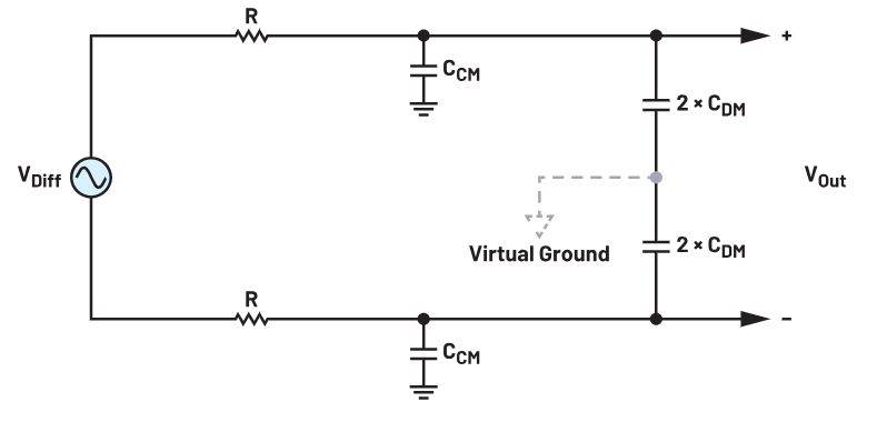
Figure 1. Balancing cm-dm emi filters (emphasis on false locations)
01 misreading falsely
Fiction concepts are often taught when introducing discharge circuits. In fact, the concept has been repeatedly used and explored in practice, and its essence is often blurred or forgotten。
If more applications of the dot model (including the dots) are not known, engineers may believe that the dots exist only at one of the input nodes of the discharge circuits using negative feedback. This is not the case, however, and this paper will be followed by a semi-circuit analysis of the cm-dm emi filter。
The circuits shown in figure 2 are a typical example of what is commonly used to describe the concept of false lands. Unfortunately, the opposite nodes of ideal negative feedback circuits are often directly marked as false. The fact is that the reverse node of the ideal negative feedback circuit has a virtual fixed level, which in this case is the local level. This point is not a bogus per se, but a node with a mirage。
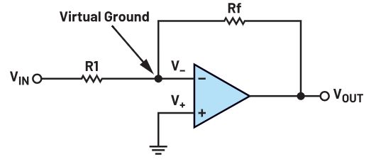
Figure 2. Optimal discharge circuits (emphasis on location of void)
According to the ideal delivery model, the input-end meets v+ = v – due to the introduction of negative feedback and the enormous gain in the opening of the ring. When the peer of the same input is located, the electrical level of the reverse input end is equal to 0 v (geographical level) by means of a short and short feature。
Figure 3 shows an example of an ideal electro-diversion circuit. In this circuit, the ideal negative feedback is a reverse node with a vdc dot. Similar to the previous example, the reverse node also exists at this time. This design method is often used for single power systems that require a dipolar signal range (e. G. ±2. 5v) or as a buffer voltage source。
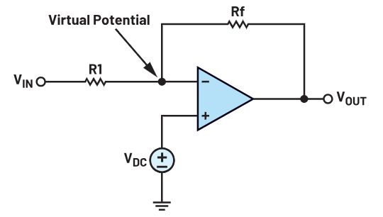
Figure 3. Optimal offsets inverse discharge circuits
02 dots and short models
Figure 4 gives a default-level model. Only very small currents can flow past model electrical resistance (r1) due to resistance to infinity. Therefore, both ends of r1 are virtually non-existent. As a result, the r1 ends are short and the dot output end is vvp。
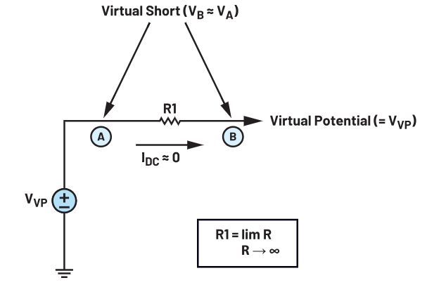
Figure 4. Optimal default-bit model
03 is infinity too idealistic
Engineers and designers are often confronted with physical conditions: resistance is endless and essentially a road. This appears to be in contradiction with the default level model presented here, but the rationale can be illustrated by a very high resistance。
In fact, theorists and teachers of the circuit simplified the concept quietly, and we were unaware of it. As students, we may be too simple to realize what it means to have an infinite resistance at the ideal input end: “the input end of the amplifier is the road?” we have thus accepted this set-up and are satisfied with the conclusion that the input end is short in the negative feedback structure. Perhaps from a more intuitive and understanding perspective: in negative feedback circuits, one input end of transport mirrors the level of the other input end (there will be some disorder in the actual circuit)。
The ideal default-level model given here helps to understand the nature of the short and the low, and the model can also be adapted for circuit simulation. The use of high-resistance resistance can achieve near-deficit levels. In general, bottlenecks are in the compressivity of the emulator, which can be addressed by selecting the resistance value and/or adjusting the tolerance of the analogue node (e. G. Reltol, etc.). Figure 5 gives an example of a circuit containing a dotted bit in a straight flow simulation of lt spice。
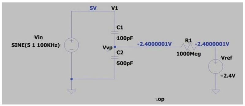
Figure 5. Lt spice simulation of the dot model
Note: in circuit simulations, the designer is in fact applying a node model whenever he uses a mega-european-scale major resistance to land (or connect to other levels) to avoid the loss of floating nodes。
Figure 6 highlights an interesting phenomenon: whether ideal or not, the dot model itself is embedded in the delivery model. Although this is not usually the case, the application of a voltage level at the (+) node of the discharge is linked to the ideal delivery of the infinity of the input resistance. Infinite input resistance, combined with negative feedback structures, has created a fissure, thus placing (-) nodes at the vdc dot。
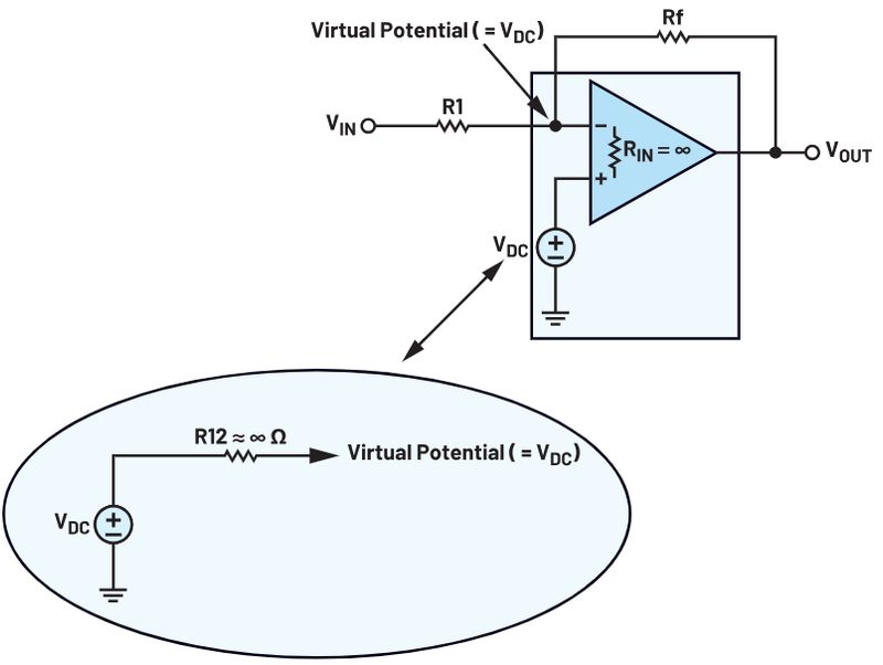
Figure 6. Fault-level models and ideal delivery models
For non-optimal delivery models, opening-entry resistance is often significant. Through the introduction of negative feedback, these resistances are further increased, and the increase is similar to the liberalization of the ring gain (rin ≈ aol x r12). Although not infinity, its extremely high input resistance is consistent with simulated dot models。
04 semi-circuit analysis, bottling and cm-dm emi filter
In the introductory part of this paper, figure 1 shows the intermediate steps of the emi filter semi-wire analysis shown in figure 7, with the aim of indicating where it should be applied. This section will present a complete demonstration of the semi-circuit analysis process, clarifying how this method can simplify mathematical extrapolation and thus determine the communication characteristics of the circuit more quickly。
In essence, the semi-wire analysis is to split the circuit into two mirror symmetric circuits. The two mirror circuits represent the same single-end circuits with the same transmission function for the differential signal. When half-wires are analysed, only one (more simple) single-end circuit can be retained for analysis. Components that are linked to both differential lines need to be modified and used as false reference points。
The semi-wire analysis uses symmetrically balanced circuit structure, opposition terms input signals and superimposed theorem. Simplified semi-wires can be used to analyse the coming or differential working state, respectively。
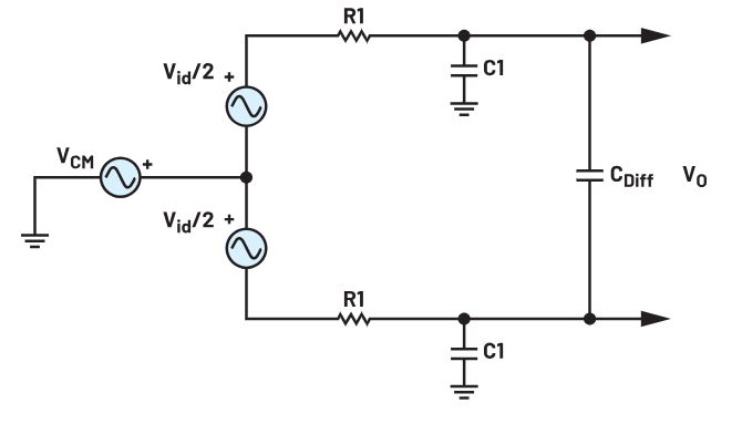
Figure 7. Cm-dm emi filters with co-mode and differential mode input signals
Note that this input signal configuration is often used in the analysis of instrument amplifiers and differential amplifiers to obtain a common and a differential transmission function, respectively。
Figure 8 redraws the filter and marks the symmetric axis. It was then divided into two mirrors. Please note that the total capacity of these two cascades is equivalent to the original differential capacity cdiff。
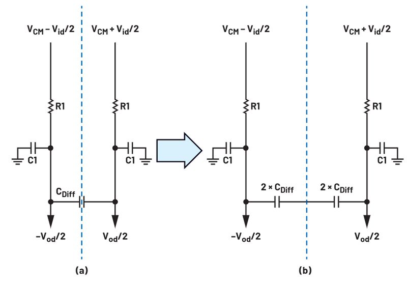
Figure 8. (a) redrawn cm-dm emi filters and symmetric axis lines; (b) replace cdiff with emi filters after two cascades device
Next, figure 9 shows the equivalent of co-modes and differential mode semi-wires. It needs to be noted that the commodular half-wires are available through all half-wires that are disconnected. The differential half-wire is obtained by connecting all half-wire interconnection points to the vantage point。
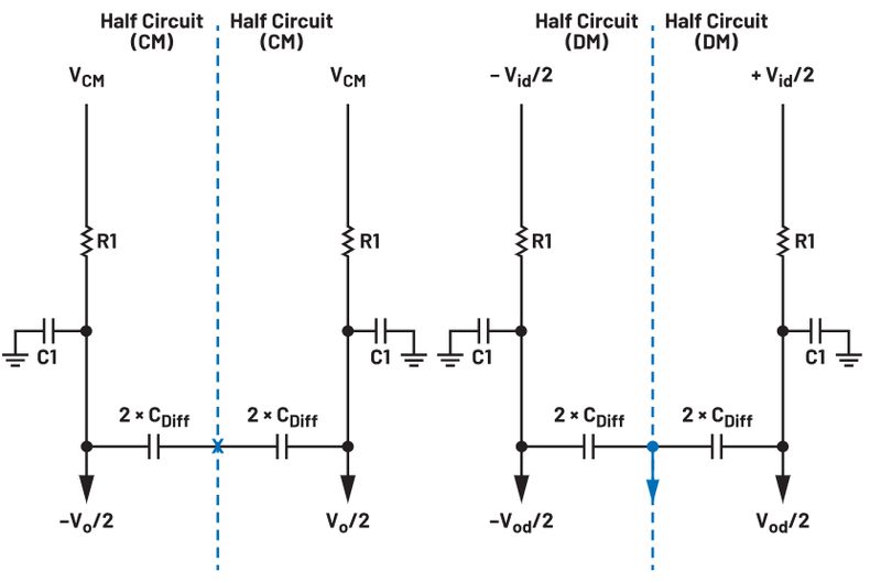
Figure 9. Coming and differential model semi-wires
The last step would be to replace the void with a signal. Despite the infinity of resistance, the other half of the differential circuit can be effectively inhaled or drained, as shown in figure 10a. This has the same effect as the signal: a ground level node capable of inhaling or running electricity。
In a circuit transfer function extrapolating or imitating, a vantage point may be substituted for a signal location. As a result, two combined capacitors can be directly combined and obtain a simple rc circuit, as shown in figure 10b。
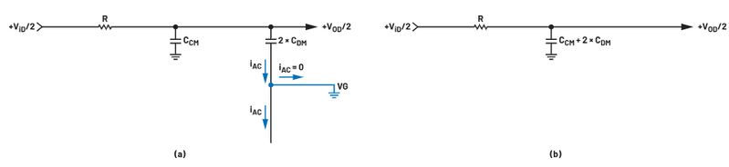
Figure 10. (a) visible dm circuits; (b) fusion is replaced by circuits behind signals
Using these simplified commodules and differential mode semi-wires, you can extrapolate the cm and dm transfer functions and their corresponding bandwidth expression. For reference, figure 11 shows the equivalent of cm circuits, dm circuits and their balanced bandwidth。
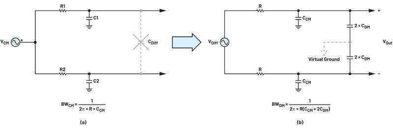
Figure 11
05 orbital subvoltage circuits and wasteland
Orbital subvoltage circuits are often used to generate bipolar power from single power sources such as batteries. A typical circuit produces a mid-point baseline voltage between power tracks using a sub-orbit structure such as an electrical resistance subpressor. In figure 12, the circuit provides the output current, while the output level is stabilized at batt/2 at a no-go level through negative feedback buffers。
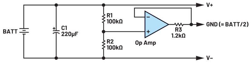
Figure 12. Orbital subvoltage circuits
Note: v+ level batt/2 and v-batt/2 relative to local level vgnd。
Unfortunately, on a number of occasions, the medium-orbit sub-voltage circuits have been mistook as the vantage circuit. Since the orbital sub-voltage circuit is designed to be capable of exporting and inhaling currents, its output node is not false but is a real node with a circuit for the return of currents. Such misnamed names can easily lead to confusion in the understanding of the dots, including the dots。
“... Is a false notional node of a circuit that can be maintained at a local level without direct connection.”
The concept of a dotage level does apply to the circuit, as evidenced by the shortness of the buffer amplifier, which obtains a subpressure level from the battery. However, the entire circuit does not provide a real void。
Conclusion
The application of the concept of dots and dots is not limited to the distribution of negative feedback circuits, but can also simplify more circuit analysis. In fact, these models can be used in many scenarios, both to deepen the understanding of the principles of circuit work and to simplify mathematically significantly。