During the development and production of semiconductor chips, in addition to the well-known optical carving machines and corrosive machines, there is also a core precision device that appears to be low-key but indispensable - a probe。
It can be said that without a probe, there is no chip performance test. Whether it is a 5g/6g radio frequency chip, a third generation semiconductor sic/gan power device, or quantum material, photocommunication chip, all crystal circle-class electron performance, high frequency parameters, high temperature reliability tests, cannot be detached from the precision of the probe。
In recent years, with the acceleration of the process of domestication of semiconductors, the market of probes, once monopolized by overseas brands, has now ushered in a full-scale siege of domestic equipment, with domestic manufacturers, represented by sengdongbao technology, replacing imported equipment in all its aspects。
I. Central role of the probe: “exact medical examiner” of the chip
A lot of people wonder what the needles do
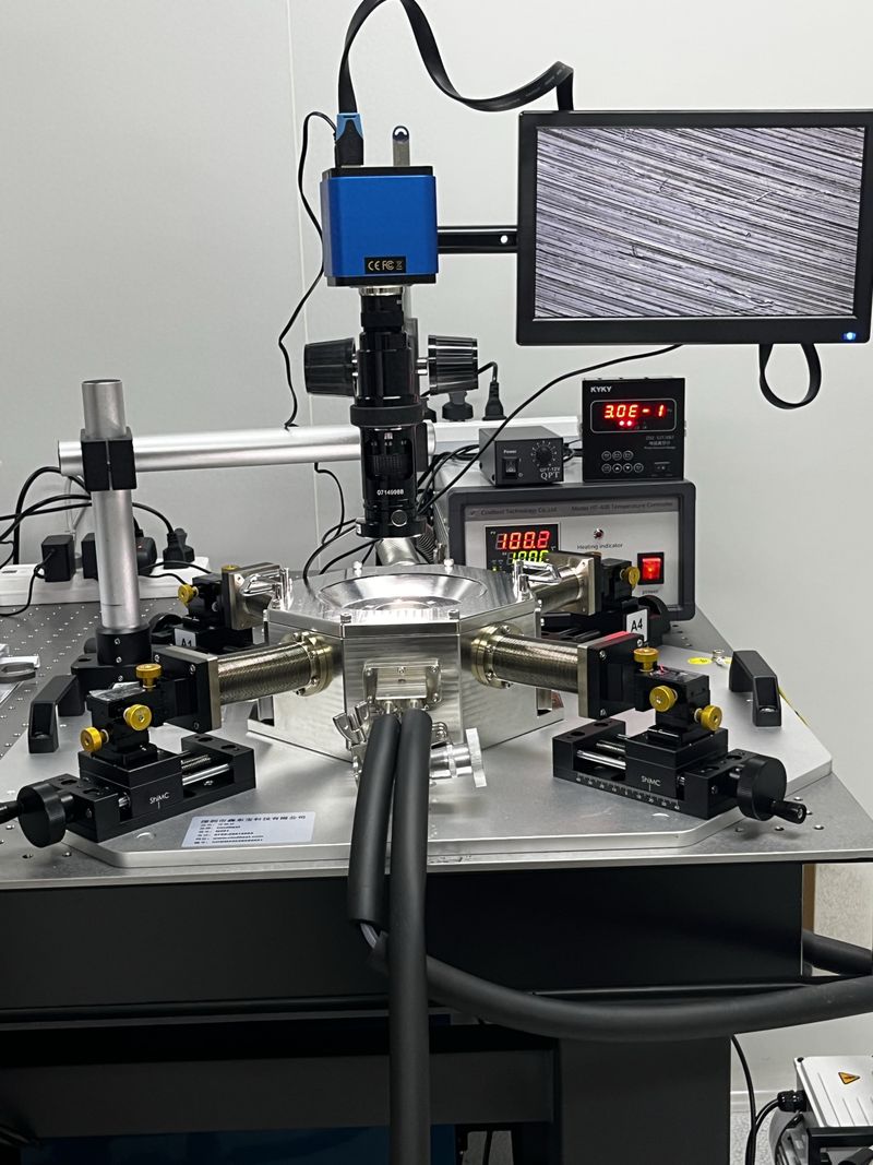
In short, the probe is a non-destructive test precision device. The full-dimensional performance test is completed by means of a high-precision probe-driven micrometer probe, a small welding disk with precise contact with the chip's crystal circle, the export of internal telecommunications, radio frequency signals, light telecommunications, equipment such as analysers, source forms, etc. Within the chip。
It runs through the whole industry chain of chips:
Chip design phase: certifier device parameters, optimize design options
Crystal round manufacturing phase: screening of bad crystal circles to improve production performance
Encapsulation testing phase: testing the reliability of the chip, removing the failed product
Research and development phase: to meet extreme environmental tests such as high and low temperature, vacuum, high frequency
A high-quality probe directly determines the accuracy of the chip test data and is the core hardware support for advanced semiconductor development and forward material scientific research。
Ii. Mainstream probe classification, covering the needs of the whole scene test
Based on the degree of automation and testing functions, the needles currently available on the market are divided into four main categories, corresponding to the whole scene needs from higher education research to industrial production:
Manual probes station
A streamlined structure, high value for money and easy to operate, with the manual fine-tuning of the probes to complete the position tests and fine-tuning of the calibrations to the level of the μm. The tests of basic equipment for small enterprises, which are applied mainly to higher education laboratories, teaching experiments at scientific research institutes, are the first option for semiconductor testing equipment at the entry level。
2. Semi-automatic probes station
The current market mainstream bursting machine type, with a motorized migration platform, supports a crystal circle automatic scanning and point-to-point double testing. The high-temperature modules can be added to the test capability of dc ~110ghz full-band radio frequency, which is widely used in the medium-test development of 5g/6g radio-frequency chips, silicon-ray chips and third-generation semiconductor devices, with a high-value advantage。
3. A fully automated crystal probe station
High-end equipment for industrial mass production, with a large 8-12-inch crystal circle, with a visual automatic alignment system, allow for bulk automation testing, automatic data acquisition, the distribution of electromagnetic shielding structures, the effective circumvention of external signal interference and the need for large-scale production testing for the head semiconductor enterprise。
4. High cryogenic vacuum probes station
High-end scientific equipment is also the advantage of the differentiation of national production equipment. An integrated test of a very low temperature of 4. 5 k to 675°c, a high vacuum environment, which addresses pain points such as cryogenic frost, signal drift, sample oxidation of traditional equipment, extreme environmental reliability tests for assigned amount sub-units, superconductors, vehicle grade power units, etc。
Iii. The pain in importing equipment has been highlighted, with the introduction of a national probe to replace the wind
For a long time now, the domestic market for high-end probes has been monopolized by overseas brands, but the disadvantages of imported equipment have become more apparent: expensive equipment, long delivery cycles of several months, high late maintenance costs and poor customization capacity have greatly constrained the progress of research and development in domestic semiconductors and research institutions。
With a breakthrough in sophisticated domestic manufacturing technologies, the national production needles have completely broken the technical barriers. In shenzhen city, for example, cindbest, a state-owned high-tech, specialized and new enterprise in the deep-farming industry for more than a decade, has achieved 100 per cent ownership of the core components of the probe。
From radio frequency probes, high-precision probes, to vacuum cavities, temperature control systems, shielding structures, all self-generated, free of overseas supply chain constraints. The equipment performance is high-end, but procurement costs, delivery cycles, and after-sale protection are generally better than imported equipment, making it the preferred choice for many higher education institutions, research institutes and semiconductor enterprises。