
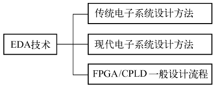
1. 3 eda technology
Knowledge division network
1. 3. 1 electronic system design methodology
With the development of programmable logical devices, particularly after the 1990s, the development and diffusion of eda technology for electronic design has revolutionized the design methods and means of design of digital electronic systems. The traditional bottom-up (bottom-up) design based on circuit boards has evolved into a chip-based top-down (top-down) design。
Traditional electronic system design methods
Traditional electronic system design is generally based on circuit board design, using a bottom-up design approach. The design of the system hardware begins with the selection of specific logical metaware, which are used for the logical circuit design, the completion of the individual functional modules of the system and the linking of the functional modules to the complete hardware design of the system as shown in figure 1. 59。
From the lowest level to the highest level, the design method is called " bottom-up " . The main features of this design approach are:
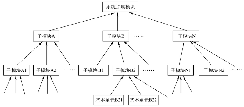
Figure 1. 59 top-down mapping of design methods
(1) introduction of common logical metaware
(ii) simulation and debugging at the late design of the system
(3) the main design document is the electromechanical chart。
Using traditional design methods, designers familiar with hardware, with their design experience, can complete the design of sub-circuit modules in a very short period of time. The lack of overall functional control of the system by the general designer has led to a longer period of time required to package the various submodules to complete the system's commissioning to achieve system-wide functionality and to a higher level of collaboration among designers using this method。
2. Design methods for modern electronic systems
In the early 1980s, computer-aided design technology (cad) was introduced in hardware circuit design. Initially, only computer-based software was used to create the wiring of the printing boards, which was followed by the design and simulation of an electronic circuit of a plate size of the plugin。
With the development of the large programmable logical device fpga/cpld and the emergence of various emerging eda tools, the traditional circuit board design has begun to shift to chip-based design. A chip-based design not only achieves multiple digital logical system functions through chip design, but also significantly reduces the workload of circuit chart and panel design, increases design efficiency and enhances design flexibility, while reducing the number of chips, reducing the size of the system and improving the reliability of the system. Thus, a chip-based design approach is now being mainstreamed into the design of modern electronic systems。
A little hint
From the previous practice, we know that the tools and devices necessary for the design of the chip are computers, programmable logic devices (fpga/cpld) and eda tool software. The above conditions have made it possible to complete the design and production of digital systems in laboratories。
The new chip-based design is based on a top-down (top-down) design approach, which is based on the overall requirements of the system, progressively fine-tuning the design from the top down and finalizing the overall design of the system hardware, as shown in figure 1. 60。
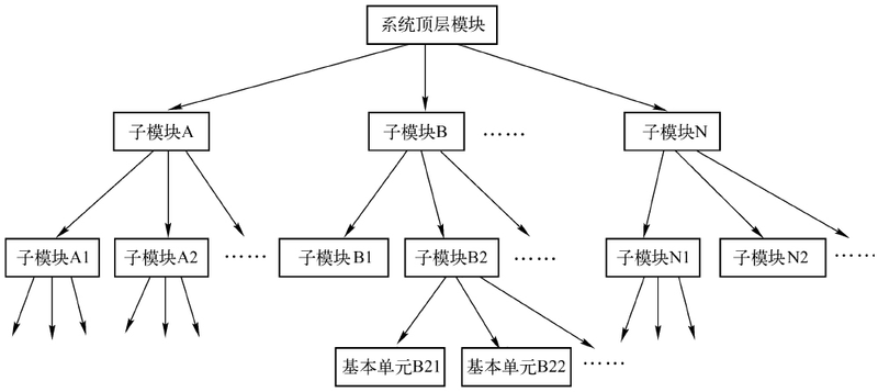
Figure 1. 60 map of top-down design
The main features of this design approach are:
(1) more rational, open and standardized circuit design using fpga/cpld
(2) use of system design for early simulation
(3) the main design document is the hardware desSource program prepared by cription language。
Using this design approach, the system analysis, the overall validation of the system programme was completed at the beginning of the design cycle, the system was divided into several operational modules, tasking and indicator allocation, functional simulation and debugging of higher-level modules, which enabled early detection of structural design errors, avoidance of waste of design work, help to designers avoid unnecessary duplication of design and increased the success rate of design。
1. 3. 2 fpga/cpld general process for circuit design
The fpga/cpld circuit design process is a computer-based development design process for fpga/cpld devices using the eda tool software, which typically includes design preparation, design input, functional simulation, design realization, time-series simulation, download programming and device testing, as shown in figure 1. 61。
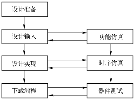
Figure 1. 61 fpga/cpld general process for circuit design
1. Design preparation
The design preparation phase is the first step of the fpga/cpld in the design of the circuit, including the validation of the programme, the design of the system and the selection of the device。
2. Design input
The design input phase is where the designer enters the design circuit in some way into the computer. Design input usually takes the following forms: theoretical chart input, hdl hardware description language input, wave input, hierarchical design input, status chart input, etc. The first two are more common input methods。
(1) the method of input of the schematics, similar to the traditional schematics, describes the design circuits in the most direct graphic manner, uses the symbols in the matrix provided by the tool software, and draws the syllables by wire. This type of input is one of the most common ways to visualize and facilitate simulation, but it is inefficient and demanding for designers。
(2) hdl hardware describes the language input mode, text-based input of the design circuit, which is one of the basic features of the eda design. Vhdl (very high description des) is currently used in the description of hardwareI'm sorry. Because language is not related to process, this way of entering design circuits does not require designers to be too familiar with bottom circuits and pld structures and facilitates the design of large-scale systems; the disadvantage is that the hardware description language has to rely on composites, whose good or bad effects directly affect the quality of the circuits generated。
3. Functional simulation
The functional simulation is also known as the pre-impression. A logical function check of the design circuit is performed prior to compilation and a preliminary test of whether the circuit function is correct. Simulation starts with the creation of waveform files or test vectors, and the simulation results are typically output signal waveforms and report files, etc。
4. Design achievement
When the logical function of the design circuit is correctly verified, it will be able to enter the design realization of the circuit. Design realization is a key step in the design of the fpga/cpld circuit, and the tool software will logically streamline, synthesize and adapt the design input files (principle maps, text, etc.) and eventually produce the programming files required for programming downloads。
5. Time-series simulation
Time-series simulations, commonly referred to as behind-the-simulations, are simulations that combine the design circuits with the fpga/cpld. Because of the different delays in the internal parts of the different devices, different layouts also create different delays. Therefore, the time-sequencing really adds to the simulation of the design circuit after the delay information, when it is realized in the device and works as a real device。
Download programming
Download programming is the loading of a programming file generated during the design realization phase into the target device fpga/cpld, i. E. The design circuit will be achieved in the specific device。
7. Device testing
The device test means that, once programmed, the device can be verified, encrypted, etc. By means of a compiled document, and, of course, an on-site test of the performance of the device using the experimental plate is necessary。
Combination and summary of knowledge
The chapter, which begins with a simple digital system design mission, describes the soft and hardware environment and basic design processes designed by modern digital systems and is becoming familiar with the use of the quatus ii software in practice. It establishes a process of understanding of programmable logical devices from external to internal, from intuitive to abstract, and lays the foundation for learning from the latter chapters。
The focus of this chapter is as follows:
Topic 1
I. Filling in the question
1. Conversion between digits。
(1)(25)10=()2=()16
(2)(10101)02=()10=()16
(3)(3f)16=()2=()10
The design steps in task 1 include the following five steps: , , and 。
Quartus ii is a new generation of eda design tools for the company, which evolved from its earlier maxplus ii。
4. In chronological order, the programmable logic device has undergone approximately the following stages of development: , , , , 。
Programmable logical devices can be classified from integrated density into and 。
The programmable logical devices divide them structurally into two main categories: and ; and the simple programmable logical devices are structural units。
The basic structure of a simple programmable logical device consists of , , and 。
The basic resources of complex programmable logical devices consist of four parts, , and 。
The chinese meaning of eda is , which is composed of the initials of the following three english words: , and 。
The chinese meaning of hdl is and is composed of the initials of the following three english words: , and 。
11. The following abbreviations in english are translated into english and chinese。
Pla
Pal
Cpld
Vhdl
Lut
Lab
Cad
12. Write the chinese meaning of the english words below。
(1) project (2) wizard
(3) device (4) package
(5) pin (6) family
(7) schematic (8) diagram
(9) block (10) symbol
(11) input (12) output
(13) communication (14) message
(15) anallysis (16) synthesis
(17) fitter (18) assembler
(19) report (20) waveform
(21) node (22) simulator
(23) factional (24) timing
(25) assignment (26) fuse
(27) interconnect (28) macrocell
(29) produc terms (30) carry
Questions and answers
1. Draw a complete design process for quartus ii software。
Brief description of the design steps in task 1。
3. The basic structure of a simple programmable logical device is illustrated by a graphic。
Draws the input/output structure and true value tables of the 4-option 1 data selector。
Briefly describe the general design process of the fpga。