


2. 9 field effect tubes and their magnification circuits
The field-effect transistor abbreviation tube, a commonly used semiconductor device with extremely high input resistance ranging from 109 to 1014 times, has the advantages of small noise, good heat stability, low power consumption and easy integration, and is therefore widely used in large-scale integrated circuits。
The transistor tubes described above control the current ic of the collector electrode using the ib current, which is the current control element; the field effect tube controls the leaking electrode id using the grid power ugs, which is the voltage control element. Transistor tubes are the conductor of two streams, electronic and hollow, and are called bipolar transistors, while field effect tubes are directed by most of them, i. E. Only one of them is involved in conductivity, so they are called unipolar transistors。
There are two types of field effect tubes: a condensed field effect tube and an insulation fence effect tube. Limited in length, only a brief description of the application of the wider insulation fence effect tube is provided here。
2. 9. 1 insulation fence field effect tubes
Insulation grid field effect tubes can be divided into two categories, n- and p-, depending on the channel, each of which is enhanced and depleted. An example of the structure, working principles and characterization curves of the two field effect tubes is given in the n ditch。
The structure of the n-channel enhanced insulation fence effect tube, as shown in figure 2-48 (a), is lined with a single p-type thin silica, which spreads two n+ areas as source poles (s) and leaks (d), generates a sio2 insulation on the silica surface, and the metal insulation is extremely fenced (g). Because the fences and other electrodes and conductive trenches are insulated, they are referred to as insulated fence field effect tubes, or metal oxide semiconductor effect tubes, or mos tubes。
At work, conductive circuits are formed between leaks d and source poles, known as n. Owing to the number of ions mixed, there are differences in jobs divided into depletion nmos tubes and enhanced nmos tubes, the symbols of which are shown in figures 2-48 (b) and (c), respectively. If the symbol in the figure is in the opposite direction, it is indicated that the p trench draining pmos tube and the enhanced pmos tube respectively。
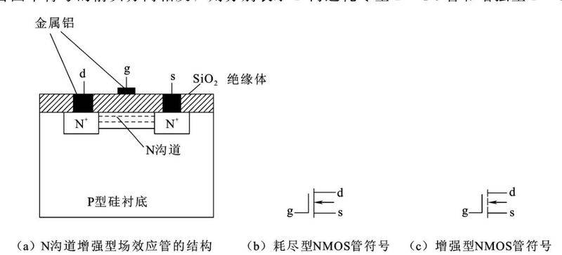
Figure 2-48 nmos tubes
1. Rationale
When ugs = 0, the diodes d and s are based on two inverse serial pn knots made up of semiconductor n-p-n and therefore leaking polar current id = 0 can be considered. When ugs > 0, the electrons in the p-lined substrate are attracted to the surface layer to form the n-type thin layer, the n-type conductive circuit. When a channel is formed, a positive voltage between the d and s poles will leak the eid. This mos tube has no conductive circuit at ugs = 0, and only when the ugs is increased to turn on the voltage ugs(th) can it be formed as an enhanced nmos tube. In the ugs>ugs(th), as the power of the fence changes to ugs, the id changes, which is the barbed control of the enhanced mos tube。
2. Characteristic curves
(1) transfer characterization curve. The transfer feature is the control character of the output current id for the input of voltage ugs at certain times in uds. While uds may have an impact on the transfer properties at the same time, in the work area of the acw, id is almost unrelated to uds; the transfer characterization curves corresponding to different uds values are almost overlapping and are usually expressed in only one curve, as shown in figures 2-49. The control of leaking electrical currents is more clearly demonstrated by the transfer properties curve, so the field effect tube is a voltage control device。
(2) the output characteristics curve. The output feature curve refers to the relationship curve between the leaking polar current id and the leaking source voltage uds at certain times of the ugs, as shown in figure 2-50. The id can be divided into variable resistance areas, constant flow areas and clipping areas to observe changes in ugs. The field effect tube is used to work in a constant-flow zone when the circuit is amplified. In this area, id is almost unrelated to uds and controlled by voltage ugs. Controlling a large current with a small voltage is the greatest feature of the field effect tube。
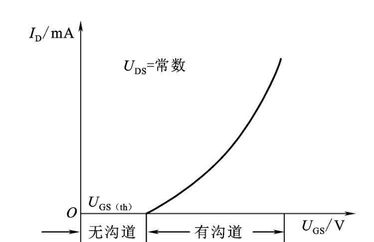
Figure 2-49 transfer characterization curve for enhanced nmos tubes
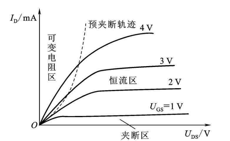
Figure 2-50 output characterization curve for enhanced nmos tubes
3. Main parameters of the field effect tube
(1) combination of voltage ugs(off). When the uds is constant and the id is equal to a weak current (e. G. 50 μa), the voltage between the grids is referred to as the breakup of the voltage ugs (off)。
(2) turn on the voltage ugs(th). When uds is constant, there is a ditch that connects the missing and source poles with the smallest ugs value, known as open voltage ugs(th)。
(3) saturation leak idss. When ugs = 0, and
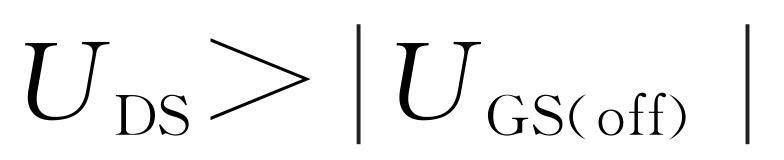
It is called saturated leak idss。
(4) direct current input of resistance rgs. The ratio of fenced voltage ugs to the corresponding grid current ig, called direct current input resistance rgs。
(5) low frequency cross-guide gm. When uds is constant, the ratio of leaking eid to grid-based voltage ugs changes is referred to as the low frequency cross-conductor, indicating that
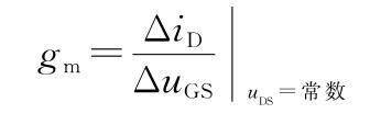
Cross-guide gm represents magnification capacity, similar to the current magnification factor of the transistor。
4. Notes
(1) because of the high import resistance of the mos tube, the polar induction charge is not suitable for release, which can result in high voltage and damage to the insulation. Therefore, when used, the fence is extremely impassable; while stored, short circuits are essential。
(2) the condensed field effect tube failure and source extremes are interchangeable. For mos tubes, if the mos tube has been lined internally with a very short source path, it is not interchangeable or otherwise interchangeable。
(3) low frequency cross-conductors are associated with working currents, and the larger the id, the larger the gm。
The mos tube is a voltage control device. It also has three working conditions. When the voltage ui is smaller than the voltage ugs(th), no conductive circuits are formed between the leakage and source poles, the mos tube is closed, and the ditches between the leakage and source poles are about 1010 times, which is equivalent to switch breaks。
When ui is greater than the voltage ugs(th), guidance begins between the leakage and source poles. When ui is much larger than the voltage ugs(th), the mos tube is fully connected, which is equivalent to a shut-down. At this time, the smallest of the troughs between the leakage and source poles was about 1,000。
As can be seen from the above analysis, leaks and source poles in the mos tube can be used as a switch controlled by a fenced extreme voltage, i. E. When ui>ugs(th) is equivalent to a shut-down; when uigs(th) is equivalent to a switch disconnect。
Ugs(th) in this chapter, also known as uth(on), refers to the open voltage of the enhanced mos tube。
The enhanced pmos tube has a switch properties similar to the enhanced nmos tube, unlike the fenced and leaked voltage at this time, which is negative, and the activated voltage. So when |u|uth (on)|, the p groove formed, the pmos conduit, which is equivalent to a shut-down; when |ui|