1. 2 common metaware and basic circuit 1. 2. 1 transistor diodes and current circuits
The conductive performance of the semiconductor is between the conductor and the insulation, with silicon and zirconium commonly used. In order to improve the conductive performance of semiconductors, trace trivalents or pentavalents have been integrated into semiconductor materials, and semiconductors mixed with trace trivalents are referred to as p-semiconductors; the pentavalents mixed with trace amounts are referred to as n-semiconductors, while semiconductors such as diode transistor tubes are made from p-semiconductor materials and n-semiconductor materials。
(1) structure of the diodes
Combining p and n semiconductors with special processes creates a thin charge area known as the pn knot on their interfaces。
Encapsulating pns in outer casings and drawing out two electrodes at two ends, respectively, constitutes a diode, with the electrode connected to p being called a positive pole of the diode and the electrode connected to n being called a negative pole of the diode. The outer shape of the diodes is many, and positive and negative polarity can be judged by the hues, colours and symbols on the outer casings, with negative polares on the one end of the colour or dots。
(2) single-directive electrical characteristics
The diodes have a single directional conductivity, and when they are positive, the diode conductivity, as shown in figures 1-18, is reduced to 0. 6 to 0. 7 v for the silicon diodes and 0. 2 to 0. 3 v for the cylindrical diodes. When the reverse bias occurs (i. E., negative, negative, positive, positive) for the diode, the end of the diode. When the reverse voltage is increased to a certain value, the diode is suddenly retroductive, a phenomenon known as reverse penetration. When an ordinary diode is struck in reverse, damage is caused and it cannot be used; while a steady diode is a special case, it works in a reverse blow-out and does not damage。
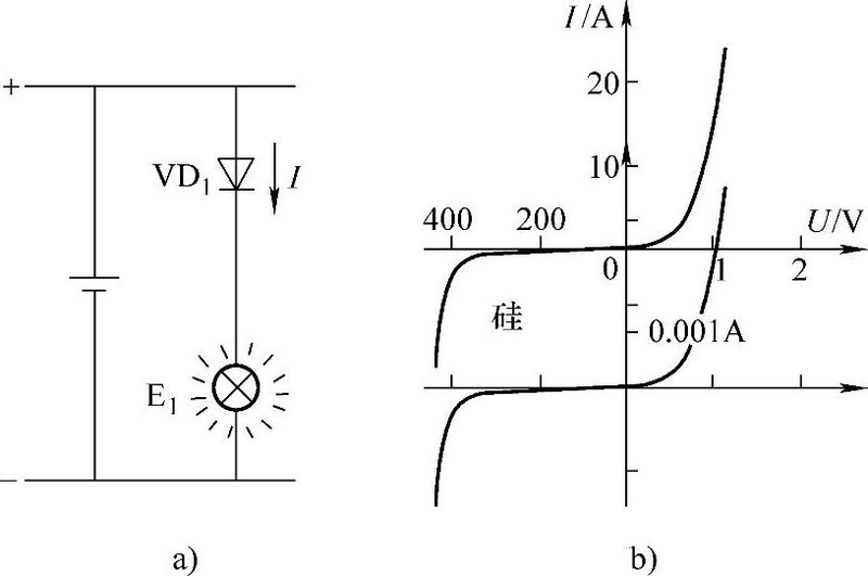
Working characteristics of diodes
(a) positive wizard b) characteristic curve
(3) fluid
The process of transforming the exchange into a single-direction direct current is called the whole current. The currents are more widely used in vehicle circuits, such as power exchanges from generators, which can only be supplied for direct-flow loads only after the currents, filters and steady pressure have become constant currents, and batteries are charged。
1-system 1-system half-wave whole-flow circuits: as shown in figures 1-19, during the week and a half of u2, the a-end is positive, the b-end is negative, the diode is positive ecstasy, the piping of the diode is ignored, the charge of both ends of the load is equivalent to u2; at the time of u2's negative half-week, the a-end is negative, the b-end is positive, the diode is inverted and the load of both ends is zero. Whole-flow circuits produce only half the waveform per cycle and are therefore called half-wave whole currents。
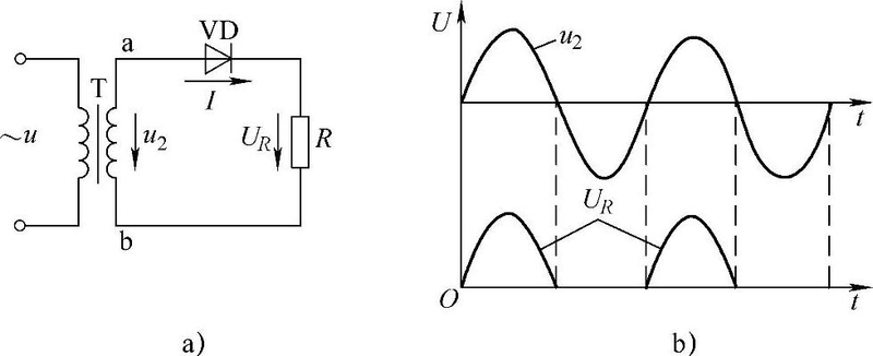
Figure 1-19 single-phase half-wave current circuits
(a) rationale b) wave graph
2 single-stage integrator currents: as shown in figures 1-20, during the first half of the week of u2, the a-end is positive, the b-end is negative, the diode vd1, the vd4 is positive and the vd3 is negative, the vd2, the vd3 is negative, the electricity flow is from the a-end and the flow back to the b-end via the vd1, r, vd4. During the negative half-week of u2, negative at the a end, positive at the b end, positive at the diode vd2, positive at the vd3, negative at the vd1, vd4, negative at the b end, current flow from the b and flow back to the a-end via vd2, r, vd3. The current direction of the overload is the same as that of the positive and negative week, and the wave shape of the voltage generated on the load is the same as that of u2. The voltage of the bridge complete output is twice as large as the half-wave。
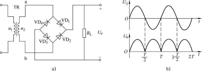
Figure 1-20 single-phase bridge complete circuits
(a) rationale b) wave graph
1. 2. 2 palliment and voltage circuits
(1) sterilization tube and its effects
The steady-pressure diode is a special silicon-diode tube with a steady pressure effect, which is used back to the circuit, works in a reverse-shock zone, and the currents of the steady-pressure tube are largely unchanged at both ends, which is the steady-pressure effect of the steady-pressure tube。
(2) steady voltage circuits
The simple, steady-pressure circuits, as shown in figure 1-21, for restricted-flow resisters and pressure tubes, are based on:
1) the adjustment process for keeping the output voltage uo stable when entering voltage is
I'm sorry
2) the adjustment process for maintaining uo stability at output voltage is
I'm sorry
It can be seen that the stability of the output voltage is automatically maintained by the adjustment of the current iz of the steady voltage tube, as long as the current iz is within the permitted range。
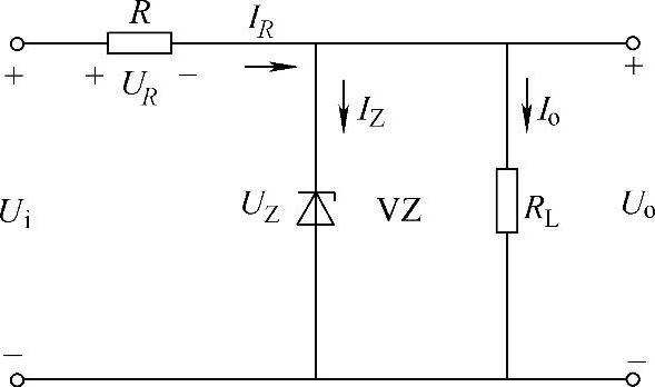
Figure 1-21 steady voltage circuits
(3) revolving diode circuits
In order to consume the self-sensitized electric motion generated by power outages in the wire, attention to the polar connection of the diodes, often reverse and resonate at both ends of the relay cycle, must be given to the polarity of the power supply, as shown in figures 1-22。
(4) other diodes
1) lighted diodes (leds): the signature of the light diodes, as shown in figure 1-23, is used in a chain of electrical resistance when the light diodes are positive in the direction of bias, and the light is transmitted and their working voltage is between 1. 5 and 3 v。
2) light-sensitized diodes: the symbol for the light-sensitized diodes is a device that converts light energy to electrical energy and is used as a coupling device in the optical transmission equipment, as shown in figure 1-24。
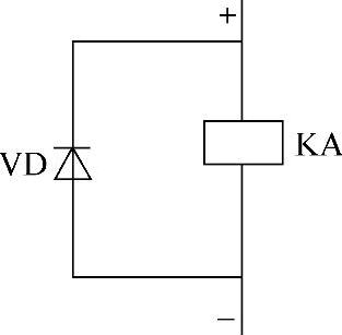
Figure 1-22 revolving diodes
Figure 1-23 optical diodes pipe
Figure 1-24 optical sensitivity diodes
(5) test of diodes
1 test using a pointer-based universal table
A. Good and bad. The pros and cons of the diodes are judged by testing positive and reverse resistance to the diodes with a universal om block, as shown in figures 1-25。
Using rx100 or rx1k to connect or reverse the two graphs, respectively, to the end of the measured diode, two electrical resistance values can be measured, the smaller of which are positive resistance, about hundreds or thousands of euros; the larger of reverse resistance, typically in hundreds of thousands of euros。
If positive electrical resistance is measured in hundreds or thousands of euros (around 10 times rx1 for cars) and in excess of hundreds of thousands of euros, it indicates that the uni-directional electrical properties of the diodes are good; if correct and reverse resistance is widespread, it means that the diodes are broken; and if correct, negative or zero, it means that the diodes are short. The latter two scenarios indicate that the diodes have been damaged。
B. Polarization. In addition to determining the polarity of the diodes from the marks of the outer casing, it is also possible to determine by measuring positive and reverse electrical resistance in the form of a universal gauge, that when the positive electrical resistance is measured, the black graph takes one end to the positive pole of the diode and the red graph takes one end to the negative pole of the diode. Because of the om block of the table, the black pen is linked to the positive extreme of the cell inside the table and the red pen to the negative extreme of the battery inside the table。
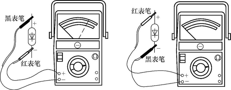
Figure 1-25 diode test
2 testing using digital universal meters
A. Good and bad. Two values can be obtained by dialling the table to the “diode test” block, connecting the two tables to the end of the diode, either straight or reverse, if the small measure is around 0. 3 v or 0. 5 v (cylinder 0. 3 v, silicon tube 0. 5 v) and the large measure is infinity, indicating that the diode is good; if both measurements are inexhaustible, indicating that the diode has broken down; and if both measurements are small or zero, indicating that the diode is short。
B. In the above-mentioned measurements, when the measured values are around 0. 5 v or 0. 3 v, the end of the red graph is a polar orthodox and the end of the black graph is a negative pole of the diode. Because of the "diode test" block of the digitized spare meters, the red pen is linked to the positive extremes of the inside batteries and the black pens to the negative extremes of the inside batteries。
1. 2. 3 transistors and magnifying circuits
Transistor tubes consist of three semiconductors, divided into two types, npn-type and pnp-type, with most common npn tubes being silicon tubes and pnp-type tubes, depending on how they are combined. Figure 1-26 shows the structure of the transistor and the symbols。
The transistor has two pn knots, one for launch and the other for collection, and three electrodes, for base (b), one for launch (e) and one for collection (c). The currents from npn-launched polar e flow are the sum of the currents from the base stage b and c; the currents from pnp-launched polar e are the sum of the currents from the base pole b and c。
1. Magnifying properties of transistors and magnifying circuits
Transistors have current magnification properties, and in order for transistor work to be in a state of magnification, they must be subject to the correct direct current bias voltage, as shown in figures 1-27, in the circuit ubb