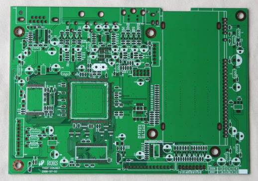
You all know that making a pcb board is turning a well-designed plan into a solid pcb circuit board, and don't underestimate the process. There are many things that work in engineering that are difficult to achieve, or what others can achieve, so it's easy to make a pcb board, but it's not easy to make a pcb board。
The two main difficulties in the field of microelectronics are the processing of high-frequency (hf) signals and the processing of weak signals, where the level of pcb production is particularly important. The same principles are designed, the same meta-devices, and the pcb produced by different people have different results. How can a good pcb board be made
Based on our past experience, we would like to share our views on the following:
- clear design targets
Accepting a design task, first, to define its design objectives, whether it is an ordinary pcb board, a high frequency pcb board, a small signal processing pcb board, or a high frequency and a small signal processing pcb board, if it is an ordinary pcb board, provided that the layout is properly organized and the mechanical dimensions are accurate. If there is a medium load line and a long line, it will be handled by certain means to reduce the load, and long lines will need to be driven, with emphasis on preventing long-line reflection。
When there is a signal line on board that exceeds 40 mhz, special consideration is given to these signals lines, such as inter-lineal interference. If the frequency is higher, the length of the wiring is more restrictive, and the interaction between high-speed circuits and their connections is a decisive factor according to the network theory of the distribution parameters and cannot be ignored in system design. As the speed of door transmission increases, there will be a corresponding increase in opposition to signal lines, a positive increase in serial disturbances between adjacent signal lines and, usually, a large diffusion of high-speed circuits, which should be given sufficient attention in making high-speed pcb。
When there are micro- and even micro-volatile signals on board, special care is needed for these signal lines, which, because they are too weak, are highly susceptible to interference from other powerful signals, and shielding measures are often necessary, otherwise they will significantly reduce the noise ratio. So that the useful signals were flooded with noise that they could not be extracted effectively。
The decomposition of the panels is also to be considered during the design phase, and such factors as the physical location of the test points and the isolation of the test points cannot be ignored, as some small signals and high frequency signals cannot be directly measured with the probes。
Other relevant factors are also considered, such as the number of plate layers, the use of a metaware containment shape, the mechanical strength of the plate, etc. Before making a pcb board, you have to be sure of the design target。
Two understand the functionality of a metaware for layout
We know that there are special requirements for the layout of special units, such as the analogue signal amplifiers used by loti and aph, and the analogue signal amplifiers require a smooth and small texture to power. Simulation of small signal components should be as far away from power devices as possible. On the oti board, the small signal is mostly fitted with a specific shield that shields the scattered electromagnetic interference。
Gl for ntoi boardThe ink chip uses the ecl process, which is very expensive and hot, and which requires special consideration in the layout of the dispersion problem, and if natural dissipation is used, the gl will be usedThe ink chips are located in a relatively smooth air flow, and the amount of heat dispersed cannot have a significant impact on other chips. Adequate attention should also be given to the possibility of serious electrical contamination if the panels are fitted with horns or other high power devices。
Three-dollar device layout consideration
One of the first factors to consider in the layout of a metaware is electrical performance, which brings together, as far as possible, closely connected metaware, especially for some high-speed lines, so that the layout is as short as possible and the power signals and small signal units are separated. To meet the electrical performance, consideration is also given to the positioning, beauty, ease of testing, mechanical size of the plate, location of the plug, etc。
Delays in transmission from and on the ground of high-speed systems are also the first factor to be considered in the design of systems. The transmission time on the signal line has a significant impact on the speed of the system in general, and the high speed of the ecl circuit in particular, although the integrated circuit block itself is very fast, it can be significantly reduced by the increase in the delay due to the use of ordinary interconnections on the floor (with a delay of approximately 2ns per 30 cm long)。
Like the moving register, the synchronous working component of the synchronous counter is best placed on the same plugin board because the transmission of the clock signal to the different plugin boards is delayed by an equal amount of time, which may result in an error by the host of the transfer depositor, and, if it is not placed on a board, the length of the clock line from the public clock source to the respective plugin boards must be equal where synchronization is critical。
Four pairs of wiring
With the completion of the design of the otni and the stellar fibre-optic network, more than 100 mhz of high-speed signal lines will need to be designed in the future, and some basic concepts of high-speed lines will be introduced here。
Transfer line
Any “long” signal route on a printed circuit board can be considered a transmission line. If the transmission of the line is delayed much shorter than the signal rises, the reflection of the owner during the signal rises will be submerged. There is no overstretching, backstretching and ringing, and for most mos circuits at present, the line can be long in rice without a signal distortion, as the increase time is much greater than the delay in the transmission of the line. For faster logical circuits, especially hypervelocity ecl。
In the case of integrated circuits, the length of the line must be significantly shortened in order to maintain the integrity of the signal, without other measures, because of the speed at which the perimeter is growing。
There are two ways in which high-speed circuits can work on relatively long lines without serious wave-form distortions, and ttl uses the shortki-diode-standing approach to fast-down edges, resulting in overstretching at a level lower than the local level of a diode voltage, which reduces the back-spill range, with a slower rise margin allowed to pass, but it is reduced by relatively high output resistance (50-80 times) to circuits in a “h” state. In addition, because of the high level of resistance in the "h" state, the problem of backlash is less prominent, and the effect of improvements in the hct series would be more pronounced if combined with the shortki-diode slot and the chained electrical resistance。
When there is a fan along the signal line, the ttl method described above appears to be somewhat inadequate at a higher bitrate and a faster edge. Because there is a reflection wave in the line, they tend to be synthesized at a high bit rate, leading to serious signal distortion and reduced resistance to interference. Thus, in order to address the problem of reflection, another method is usually used in the ecl system: linear resistance to matching. In this way, the reflection is controlled and the integrity of the signal is guaranteed。
Strictly speaking, the transmission lines are not much needed for conventional ttl and ccos devices with slower edges. For high-speed ecl devices with faster edges, transmission lines are not always required. However, when the transmission lines are used, they have the advantage of predicting the frequency of the connection and controlling reflection and oscillation through resistance matching。
1. There are five basic elements for determining whether to use a transmission line: they are:
(1) the rate of progress of the system signal
(2) connect distance
(3) capable loads (how much of a fan)
(4) resistible loads (the end of the line)
(5) percent of permitted backlash and overstep (reduced communication resistance)。
2. Types of transmission lines
(1) console cables and double winch lines: they are often used for connections between systems. The characteristics of the same-axis cables are usually blocked 50 and 75 times, while double-clause lines are usually 110 times。
(2) microband on board
Microband wires are a strip guide (sign line) separated from the ground surface by an electrical medium. If the thickness, width and distance from the ground level of the line is controlled, its characterization resistance is also controlled. Microband wires are designed to resist z0:
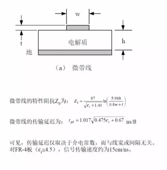
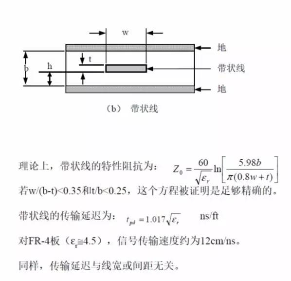
(3) lines in printed plates
A belt is a copper belt that is placed between two layers of conductivity. If the thickness and width of the line, the medium constant of the medium and the distance between the two layers of conductivity are controllable, then the characterization of the line is controllable, and the characterization of the band is resistant to:
3. End transfer lines
At the receiving end of a line, the transmission line is referred to as a conjunctivity line using a barrier end equal to the linear characteristic. It is used primarily to obtain the best electrical performance, including driver distribution loads。
In some cases, in order to save power consumption, end-to-end resistance is followed by a series of 104 capacitors forming a communication end-to-end circuit that can effectively reduce direct flow losses。
A chain of resistance between the drive and the transmission line, and the end of the line is no longer connected to the end, which is referred to as a stringed end. Long-line impulses and bells can be controlled by string-to-wire or string-to-end technologies.... Low-to-wire-to-be-to-be-to-be-to-be-to-be-to-be-to-be-to-be-to-be-to-be-to-be-to-be-to-be-to-be-to-be-to-be-to-be-to-be-to-be-to-to-be-to-be-to-to-to-be-to-to-be-to-to-be-to-be-to-to-be-to-be-to-be-to-be-to-to-to-be-to-be-to-be-to-to-be-to-to-be-to-to-be-to-be-to-be-to-to-to-be-to-to-be-to-be-to-to-be-to-be-to-to-to-be-to-to-to-to-to-to-to-。
The value of a chain of resistance at the time of the serial end is resistant to the circuit (driver door) output and the properties of the transmission line are resistant. ... There are disadvantages of a chain of links with long delays in the use of total loads and transmissions only at the end. However, this can be overcome by the use of redundant serial-end transmission lines。
4. Non-end transmission lines
If the delay in the line is much shorter than the increase in the signal, the transmission line can be used without a stringed or combined end, and if the two-way delay of a non-end line (the time a signal travels to and from the transmission line) is shorter than the increase in the pulse signal, the backlash caused by the non-end is approximately 15 per cent of the logical band. The maximum opening route approximates:
Lmax<tr/2tpd
Where: t for rising time
Transfer delay of tpd for unit long
5. Comparison of several end modes
Both end-to-end and serial-to-end connections have advantages, depending on the designer's preferences and system requirements. The main advantages of interconnection are the speed of the system and the integrity of the transmission of the signal online. The load on the long line does not affect the delay in the transmission of the drive door of the long line, nor does it affect the speed of its signal edge, but will increase the delay in the transmission of the signal along the long line. When driving a big fan, the load can be distributed along a short line of branches, rather than having to load a total online terminal as in a string-end。
The ability to drive several parallel load lines on the circuit is made possible by a serial end-to-end approach, which causes a delay time increase of approximately twice as much as the corresponding inter-end line due to the capacity load, while the short line slows the edge speed and increases the delay time for the driving door due to the capacity load, but the string-to-wire ratio of the serial end-to-wire and the connection is much smaller, mainly because the signal is transmitted by only one half of the logical size of the string-to-end connection, so that the switch-on current is only half the switch current that is connected to the inter-end。
The choice between double panels and multilayers for pcb is determined by the degree of complexity of the maximum operating frequency and circuit system and the requirements for assembly density. When the clock frequency exceeds 200 mhz, a multilayer is preferred. If the working frequency exceeds 350 mhz, it would be preferable to select the printed circuit board for polytetrafluoroethylene as an intermediate layer because its high frequency decay is smaller, its parasitic capacity is smaller, its transmission speeds faster, and because z0 is larger and its cost-effective, the following principles are required to route the printed circuit board:
(1) all parallel lines shall be kept as long as possible between them in order to reduce collusion. If there are two lines of signal in close proximity, it would be preferable to take a line between the two lines, which could act as a shield。
(2) signal transmission lines are designed in such a way as to avoid a sharp turn in order to generate a reflection in case of a mutation resistant to the characteristics of the transmission lines, and are designed as far as possible to provide a uniform arc line of a certain size。
(3) the width of the printed wire may be calculated on the basis of the characterizational resistance formula of the above-mentioned microbands and bands, and the characterization of the printing of the microband on the circuit board is generally between 50 and 120 times. To be resistant to large properties, the width must be narrow, but thin lines are not easy to make。
A combination of factors makes it more appropriate to opt for a resistance value of about 68 times, since the selection of 68 times is resistant and an optimal balance can be struck between delay time and effort. A 50-time transmission line will consume more power; while greater resistance can reduce the power consumption, it can cause a great deal of delay in transmission time。
Negative-line capacitation results in increased transmission delay time and reduced resistance to properties. However, the inductive capacity of a low-intensity segment of the line is relatively large, so the transmission delay time and the characteristic resistance to load capacity is less affected. An important feature of the transmission line with the appropriate end-line is that the branch short line should have little impact on the delay of the line. When z0 was 50. The length of the branch brief must be limited to 2. 5 cm ... In order to avoid a large ringing。
(4) four-story line for two panels (or six layers). Lines on both sides of the circuit board are to be vertically linked to each other in order to prevent the interaction of the main product。
(5) in the case of large electrical devices, such as relays, signal lamps, horns, etc., on board the printing boards, it is advisable that their landlines be separated so as to reduce noise on the surface, and that the groundlines of these large electrical devices be connected to an independent major on the plugin and backboard, and that these separate surface lines also be connected to the interface of the entire system。
(6) if there is a small signal amplifier on the plate, the weak signal line before the magnification shall be removed from the strong signal line and the route shall be as short as possible and, if possible, shielded by the ground line。