


Modern microelectronic seals, in particular electronic ceramic seals, are increasingly required for the resolution of printed graphics to the base plate and for the quality of printing, together with the miniaturization, light quantification, powerization and metalization requirements of electronic devices, leading to the development of electronic sealing techniques in the direction of high integration and density, and to the requirement of lower and higher resolution of the circuits' bar and line spacing。
In the above context, filamental printing has become an extremely important process in the production of electronic ceramics, such as thick-film ceramics (tfc), low-temperature co-burning ceramics (ltcc), high-temperature co-burning ceramics (htcc), and tablet multi-layer ceramics capacitors (mlcc), which are used extensively in the production process。
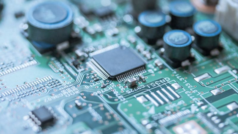
1. What is silk-net printing technology
Ribbon printing is a very traditional method of printing and is widely used in the electronics industry, the ceramics industry and the textile printing industry. The underlying principle of this technology is that part of the web-printed hole is able to pass through the slurry, while the rest of the sluice is blocked and does not create a blank on the base plate。
In the field of electronics, they are used in the manufacture of printed circuit boards, thick membrane integrated circuits, solar cells, electrical resistance, capacitors, voltage elements, photo-sensitive components, heat-sensitive elements, liquid crystal displays, etc., and are adapted in practice to new types of materials and new high-precision automation equipment, increasing the degree of process manufacturing of today's silk-net printing technologies。
Characteristics of the silk-net printing process
(1) prints of different shapes, sizes and materials may be applied, for example, to flats or to specific cones of shapes, all for materials such as glass, ceramics and plastics。
(2) wireline print layouts are soft and flexible, so they can be printed not only on soft thin surfaces but also on fragile, fragile objects。
(3) the thickness of the printed layer is easy to reconcile and is strong in stereo。
(4) applicable to different types of slurry printing。
(5) silk-net printing equipment is low-cost and can easily result in scale production。
3. Use of silk-net printing in integrated circuits
Integrated circuits can be broadly divided into two broad categories: semiconductor integrated circuits and hybrid integrated circuits, which in turn can be divided into membrane combined integrated circuits and thick membrane integrated circuits. Of these, thin membrane integrated circuits are manufactured by thin membrane technology that applies vacuum spraying, and thick membrane integrated circuits by filament-printed membrane technology。
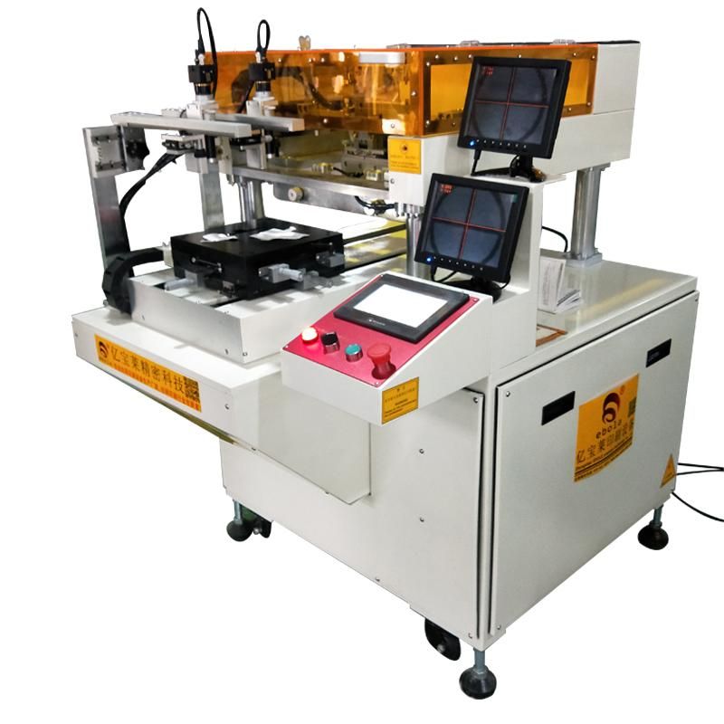
Chart. Ceramic thick membrane circuit wiring machine viabola printing equipment
The wiring image of integrated circuits is small and requires a high degree of precision, so printing machines, printing plates, printing presses (baseboards), inks, etc. Require high precision, and printing sites must remain constant and clean of dust。
4. Wire-net printing materials in thick membrane integrated circuits
(1) wire-printing
Wire-printing is the basis, using a large number of materials and processes, including the following:
One wire:
One of the main materials, commonly used nylons and polyesters, is not suitable for high-quality web-printing products owing to factors such as greater stretching, poor print graphic accuracy, and difficulty in controlling thickness. The stainless steel network has features that are uniform in diameter, consistent veil thickness, small stretch and ink-like, resulting in higher quality and adaptability of printed graphics for conductor printing in the electronics industry。
Parameters such as the number of lines, wiring paths, opening sizes and so on have a significant impact on the quality of silk-net printing。
2 bandages:
The general frame selects the aluminium frame, the bandage process directly affects the quality of the copy, and the quality element of the bandage is to control the tension。
When bandaged, the wire must have some tension, which needs to be even. The bandage is too tight to deform or torn. The bandage is too small, the wire is soft, the print is vague and the film is thin. During the bandage, the tension of the wire should be measured at all times using a tension gauge, which should be stopped and evenly transmitted when the standard tension is reached。
3 sperm:
The main requirements of silk-printed versions for sensory glue material are good layout, easy to coat, defined sensory spectrum range (uv), high visibility and resolution. The main components of the sensory glue are membrane, sensory and assistive agents。
4 scratch materials:
Scratch materials are generally polyurethane or fluorinated rubber with a hardness of 70°c ~ a80°c. In addition, in selecting the shape and hardness of the scratchboard, consideration should be given to what pattern is printed on the circuit board. In general, the blade is 90° or 60° and the plate angle is 70° or 75°。
(2) ceramic plate:
Currently, the most sophisticated ceramic foundation material for research applications is the aluminium oxide ceramic base plate, a material dominated by aluminium oxide (al2o3), which has better conductivity, mechanical strength and heat resistance. There are also ceramic panels for materials such as aluminium nitrogen, beryllium oxide, silicon carbide and boron nitrogen。
The thick film shall be made with regard to the mass, size, roughness, warp and defects and contamination of the surface of the ceramic plate and shall be washed with ultrasound between purification。
(3) slurry:
There are three types of conductor slurry, electrical resistance slurry and insulation, which typically consist of precious metals and low melting point glass. Plutonium is made with regard to its mass, viscosity and inflation factors. Slurry used in the printed thick membrane circuits consists of gold, silver, platinum, platinum, etc。
The above-mentioned metal powder is spread over organic resin adhesives and is then printed on the ceramic base. Organic resin adhesives are burned after high temperature fever, and almost all the remaining are pure precious metals, bound to the base plate by the effect of glass. This membrane can be used as a bottom metal sheet for thick membrane circuits, thick membrane electrical resistance, thick membrane capacitors and semiconductor integrated circuits。
5. Wireprinting
The general printed circuit boards, which begin with the conductor printing, repeat the electrical resistance 2-3 times, sometimes cross-printing glass coatings as appropriate, after printing, with the following processing or processing:
(1) amortization process: 5-7 minutes after printing until the end of the thread
(2) dry treatment: drying at temperatures around 100°c
(3) burning: burning at temperatures of about 650 ~ 670 °c. This process is very important, so the temperature of the furnace should be adjusted at all times to keep the temperature suitable for slurry sintering
(4) adjustments: adjustments to electrical resistance values, generally by spraying circuit boards or by lasers
(5) package: protects the built-in components。