

Original language from a specialized book: hardware design guide, from device recognition to cell phone base design
The boost booster power source, a switch to maintain a stable output by using the time ratio of switch conduits and switches, is widely used in electronics in industries with small, light and efficient characteristics and is an indispensable power structure。
In order to understand the rationale of the boost-voltage circuit, which consists mainly of basic components such as control of ic, power perception and switch tubes, the book is addressed to non-synchronous boost (synchronous boos uses switches instead of diode tubes), and figures 2-9 represent the basic boost peg。
Public backstage reply keyword: boost simulation file
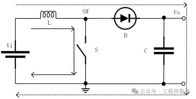
Figure 2-9 boost power surge
Similar to the buck power source, when switch s is activated, the sw point is charged directly to the x-ray l charge by a conductor. The sw voltage is 0, vi is charged directly to the x-ray l charge. At this point, the two-end voltage voltage is vi, the voltage variance is ion, the charge flow path is followed by the solid line arrow in the figure, the switch lead time = the space ratio* switch cycle = d*t, according to formula 2-1, the formula(2-13) is obtained after consolidation, and f is the switch frequency, which is the last number of the switch period t。

When switch s is disconnected, l provides load discharge via a diode tube; at the same time, vi also provides load discharge via a diode tube, discharge time = (1-1 to space ratio)* switch cycle = (1-d)*t, at which point the two end voltages are vo-vi (note: vo-vi), current variability is iof, with formulas 2-14 and 2-15. During the two periods of switch conductivity and disconnection, the charge and discharge are the same as iof=ion, which is known as the volt-second properties of the sensor。

3 within the two times of the switch connection and disconnection, iof=ion, we connect formulas 2-13 to formula 2-16 to the output and input relationship of boost, i. E. Formulas 2-17, then sorted to 2-18, which is the input output voltage calculation process of boost. As you can see from the formula, due to 0
We simulate the boost power source based on the simulation software multisim, and the simulation rationale is shown in figures 2-10. The switch frequency is 20 khz, 50% of the space ratio d, the q1-drive is the square wave of 5vpp and the bias is 5v; the electron sense is 680uh and the input voltage vi is 10v. The theoretical output voltage should be vi/(1-d)=20v. As we can see from the voltage probe, the output voltage dc is 18. 4 v, close to the theoretically calculated 20 v。
Public backstage reply keyword: boost simulation file
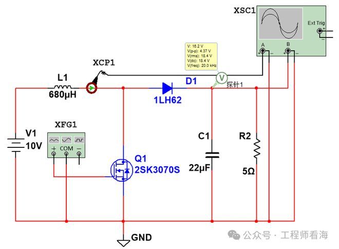
Figure 2-10 boost power simulation doctrine