

High power boost up the circuit
The voltage circuit is a circuit capable of converting low voltage to high voltage, while the boost-voltage circuit is a special voltage circuit that uses the properties of electrical senses and capacity storage to increase the input voltage to the output voltage and achieves a certain power output through external loads. This paper will provide detailed information on the working principles and design methods of the large power boost-pressure circuit to help readers better understand and apply it。
I. Rationale
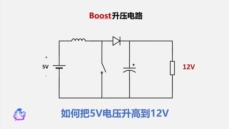
The circuit consists of the input end voltage vi, switch q1, sensor l, capacitor c, and a diode d1 and load r. When q1 is used, the magnetic field of q1 will store a certain amount of energy and transmit it to the cap c to raise its voltage; when q1 is off, the magnetic field of q1 will force the charge stream to pass through the diode d1, thereby maintaining the circulation of the charge. This results in an increase in input voltage and output of a certain power by load。
Ii. Design methodology
Large power boost voltage circuits need to be designed according to specific requirements and provide a basic design method here。
1. Determination of input and output voltage
First, input voltage and target output voltage that clearly require lifting is required. Typically, input voltage is limited to a certain extent and output voltage is designed according to demand。
2. Determination of output currents and power
Next, output current and power needs to be determined. The output current is determined on the basis of the load, and normally the output current is required to be not less than the rated current on load. Output power can be calculated by multiplying voltage and current。
3. Choice of electromagnetic and capacitive
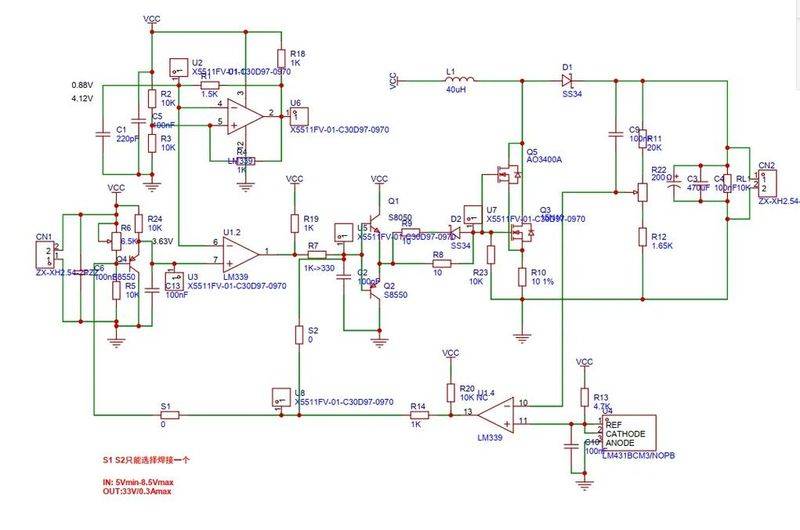
After determining the input voltage and output voltage, currents and power, the appropriate electrons and capacitors are selected according to the following formula:
L (vout x ton x d) / (Δil x fs)
C (io x d) / (Δv x fs)
Of these, l means a sense, c means an electricity, vout means an output voltage, ton means a break time for the switch, d means an empty ratio, Δil means a peak current change, fs means a switch frequency, io means an output current, and Δv means a peak voltage change for the cap。
4. Selection of switches and diodes
The appropriate switches and diodes are selected based on output currents and power. In general, switches require a high degree of conductivity, rapid response time and efficiency, and diodes require high reverse voltage and reverse current tolerance, taking into account their reverse recovery time。
5. Choice of circuit control
In the voltage circuit, the breakout of the switch pipe is done by the control circuit. There are usually two types of circuit control, one based on analog controls and the other on digital controls. Simulation control circuits can respond quickly to circuit changes, but with lower accuracy; digital control circuits are more flexible and precise, but require more complex hardware design and programming。
Iii. Example of application
High power boost voltage circuits are widely used in various electronic devices such as converters, reversers, dc/dc converters, etc. The following is an example of a boost voltage circuit design based on atmega avr single machine for readers:
1. Design parameters
Input voltage: 12v
Output voltage: 30v
Output current: 5a
Output power: 150 w
Switch frequency: 100 khz
2. Designing electrons and capacitors
Under the formula, the following are available:
Lium (30 x 1. 5 x 0. 4) / (5 x 100,000) = 1. 8uh
C ≥ (5 x 0. 4) / (18 x 100,000) = 11nf
Choose 2. 2uh for the sense and 15nf for the capacitor。
3. Selection of switches and diodes
Select irfz44n switch and mu860 diodes。
4. Choice of control circuits
Select atmega32a singles as a control circuit, using a digitally based method, using pwm channels as a control signal for the switch。
Pcb design
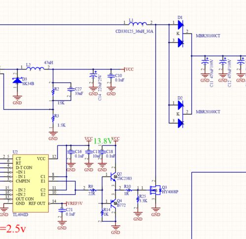
Based on circuit parameters and selection results, the design and layout of the pcb is completed, and the designs and calibration of the matrix and the pcb are prepared。
Summary
This paper provides a detailed account of the working principles and design methods of the large power boost-pressure circuit, which it is hoped will help readers to better understand and apply. In practical applications, design and selection needs to be tailored to specific requirements, with a focus on the quality and reliability of the circuits, ensuring their stability and working efficiency。