
Cpld-based fpga from and quick load programme
The field programmable gate array (fpga), as a semi-customed circuit in the specialized integrated circuit (asic) area, can be used flexibly to achieve the output of various interfaces or bus lines, depending on design needs, and is increasingly used in equipment-end communications products. Fpga is based on a static random storage (sram) structure, and reloading is required every time a post-battery program is lost. With the upgrading of the fpga scale, the capacity of the loading program has also grown, such as the 6slx150t in the xilinx - 6 series, which can be loaded up to a maximum capacity of 4. 125 mb. Among the communications products, the system is required to start quickly and the corresponding fpga is loaded for as short a time as possible, so that its loading is an issue that must be properly addressed in product design. The article describes the parallel realization of the fpga loading method through the complex programmable logical device (cpld) to meet the requirements of the communications system for a fast load and low occupancy of resources。
1 fpga common configuration
The fpga configuration data are usually stored in the system's memory, and the post-electric controller reads the bit files and loads them into the fpga, in the same manner as jtag, from a combination, from a string, from a master of four, and in the same way as different manufacturers。
(1) border scanning jtag mode. The single-board debugging phase uses the jtag model, which requires controllers, and the jtag interfaces, such as the fpga, form the chrysanthemum chain, and under this mode the controller's other functions are not available。
(2) from a string approach. Fewer i/o interfaces are used from a string load, mainly with fpga, but only one bit data can be transmitted by a configured clock at relatively low speed。
(3) primary approach. The main disadvantage of this approach is that the accompanying flash memory must be a model specified by the fpga manufacturer, and that the flash, which is a small, non-controlled flash shared, will be used on a single plate with two flash, which will increase the cost of the product and therefore the programme will be less used。
(4) by way of both. This post is part of our special coverage “fpga loading program”。
2 realization from and load
For example, the xilinx spartan - 6 series of fpgas are shown in table 1。
Table 1
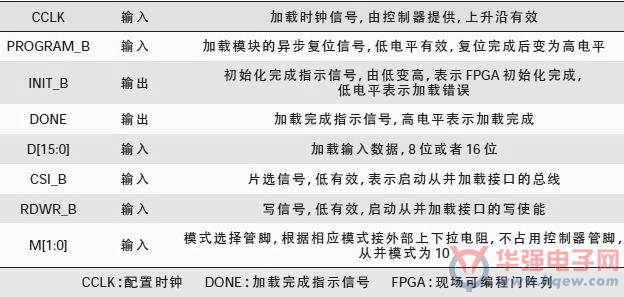
As can be seen from table 1, there are more piped resources occupied from the loading interface, and even if 8 bits are used for loading the data bus, 14 tubed feet are required. Cpus generally do not have so many general input/output (gpio) portals and are therefore used in conjunction with the loading of general and cpc files. The loading process is shown in figure 1。
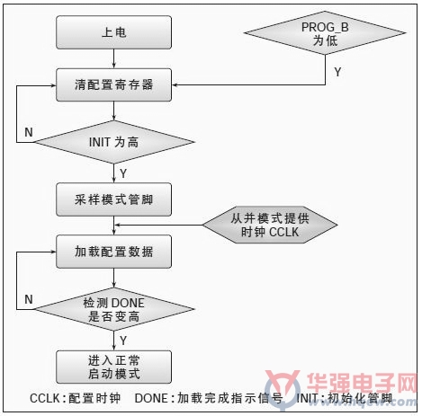
Figure 1 spartan-6 from and loading processes
3 cpld-based fpga loading scheme
3. 1 programme introduction
In equipment end-to-end communication products, fpga based on cpld has stored the configuration data in flash as shown in figure 2, and before loading the data, the cpu moved the configuration data from flash to the ddr particles by means of a local bus and double-speed memory (ddr) interface; when really needed to load, then moved the configuration data to the cpu cache via the ddr2 interface, the ddr2 interface is fast, with a clock frequency of 266 mhz, so that the one-two-step load time is negligible。
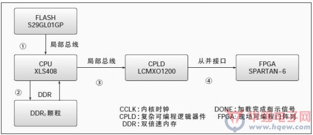
Figure 2
Cpu will then write configuration data by bytes into the cpl repository via a local bus interface with the cpl interface of 3-8 bits. In the mips series cpu xls408, for example, xls408 works at a frequency of 66. 7 mhz, which requires 10 working clock cycles at the fastest time, i. E. 6. 67 mhz, which is limited by the speed of the local bus。
When the data is written to cpcd, the data is loaded to the fpga via the interface between the interface 4-cpld and the fpga, from which the interface is synchronized with the bus and the loading time is limited to the bus clock cclk frequency。
The advantages of this programme are that: 1 and 2 paths can be processed before loading and run fast, without loading time. Loading time is limited to 3 and 4 and 3 is limited to writing bus cycle intervals and 4 is limited to clocks from interfaces。
3. 2 procedural realization
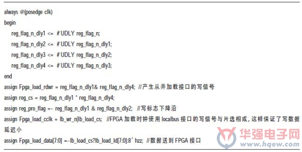
Cpcld is achieved from the co-program using the verilog language, which defines the loading module interface as follows:
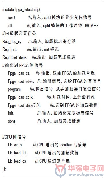
Program realization flows are shown in figure 3。
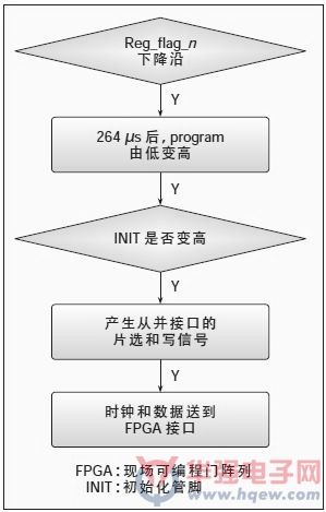
Figure 3 processes based on cpld from and loaded with fpga
The following are some of the codes produced by fpga:
4 analyze and load results
Based on modelsim 6. 5se analogue wave-forms, cpus are shown to be required to load one byte of each byte of data into the cpl, which takes a local bus cycle with a local bus frequency of 6. 67 mhz. Thus, the cpus load 4. 125 mb data to the cpl for a total of:
Cpcld requires 1 cclk byte data to fpga, cclk is generated using the letter number of the cpu local bus, which allows for the synchronization of cclk and data, resulting in a cslk clock rate of 6. 67 mhz, and therefore loads 4. 125 mb data to fpga for a total of time:
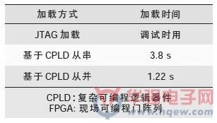
Fpga requires 1 ms, so when fpga uses 6slx150t at the top end of the spartan-6 series, the load time required on a cpld-based basis is 1. 221 s to meet the requirements of the communication product fpga load time of less than 2 s. And if you load it from a string, use the arm7 processor as a controller, for cycloEp2c35 in the neii series, configuration file size 1. 16 mb, load time takes 1. 30 min; loading fpga data with the same 4. 125 mb, using a string loading method based on cpld, when cpld loads 33 mhz, takes 3. 8 s, and the loading time of the fpga is too long, which affects the start time of the system。
Table 2 provides a comparison of the time taken to load 6slx150t-type fpga chip data, which is commonly loaded。
Table 2 fpga loading time comparison
From the above analysis, it can be concluded that if the cpu were to increase the speed of local bus writing, the time to load the fpga would be faster。
5 concluding remarks
The use of the cpld-based fpga from the loading and loading programme is of great practical value, as opposed to the other loading methods, although the loader foot has increased, but the loading time has been significantly reduced, and if the writing speed of the cpu's local bus is increased, the loading speed is further increased and the requirement for rapid start-up of the communication system is met。
Focusing on the e-commerce industry, on china's official micro-intelligence, on its fine content, and on the opportunity to get a year-round magazine
Method of concern: adding friends to search for china's powerful electronics
Or a 2-d code for "sweep."