Our usual smartphone screen consists of multiple layers of glass and electronic components to sense and process information. What does all this glass do? Today, the flopshop will analyze the cell phone touch screen structure for you。
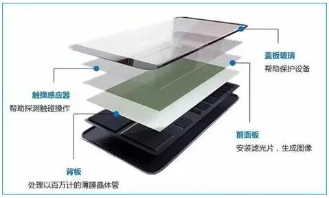
The uppermost glass is covered glass, the main component of which is silicon dioxide (sio2) and the hardness of glass in the mox table is 6. 5, which protects the inner structure of the mobile phone, but the glass is the most easily ploughed and the most painful for many mobile phone fans, so many of them prefer to have a protective film on it, the material of which is plastic film, i. E. A high molecular material, and the current mural is mainly of four qualities: pp material, pvc material, pet material, arm material。
P. P. Material has a softer membrane and a poor perforation, with no protection against scratching and wear and only dust, which is now largely abandoned by consumers because of its poor performance。
The pvc material membrane is soft and easy to paste, but it is thick, it does not perform well, and if it is torn off, it leaves debris on the screen of a mobile phone, affecting beauty。
Pet material diaphragms, which are of a high perforation, are not after they are torn off and are less likely to produce small bubbles in the middle of the diaphragms, but are of a high degree of retrospectiveness, which can lead users to lose sight of the words on the screen and can easily leave fingerprints on the surface。
The arm material, whose membrane surfaces are processed in the latest process and are resistant to grinding and scratching, has no air bubbles, is very photogenic and leaves no trace after tearing down, and is relatively the best and certainly the most expensive。
While the market is dominated by gorilla glass produced by conning, the mere use of glass-processed blues technology creates myths of market development。
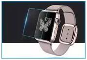
Now there's a technical substitute for glass material, and apple watch uses it. The main component of the sapphire is aluminium oxide (al2o3), which is a single crystal material and has a hardness of up to 9 degrees, and is the most solid material in addition to diamonds, which is better than glass in terms of protection against scratching。
However, sapphires are still technically at a disadvantage, such as their relatively poor resilience, which is different from hardness, and commonly known as the ability of materials to resist crack expansion. It's very important for a cell phone. The sapphire is more resilient than conning's gorilla. Even worse, the result is the use of sapphire screen phones and the use of conning gorillas. A glass cell phone is more likely to break up when it is hit or squeezed with the same force。
The second problem is light penetration. The wavelength of the visible light is 400-700 nm, and the official data from konning show that the gorillas three generations of glass have a penetration rate of over 92% for visible light, while the pass rate for visible light at different wavelengths is fairly stable. The pass rate of sapphires for visible light is less than 90 per cent, while the pass rate for visible light of different wavelengths is a circular arc curve. This raises the problem that the low rate of passivity means that the screen is even less bright when using sapphires as a cell phone lid, while the imbalance of passivity makes the screen coloury。
Indeed, for the time being, sapphires are not a perfect alternative to glass. However, in almost two to three years, there has been a considerable decline in the cost of sapphires. At the same time, a more mature manufacturing process has also allowed the sapphire screen to meet some of its current production requirements, rather than being “very low and very difficult to produce” as is rumored. Perhaps a sapphire sheet of sapphire on the face of glass could combine the advantages of glass and sapphire, while at the same time solving the problem of “hard and thin”。
The second layer is the touch sensor layer, which is divided mainly into electrical resistance and capacitation, the main function of which is to detect touch operations. The sense layer currently used is mainly an ito coated on glass with a magnetic spatter technique (oxytin oxide or tin oxide) which is a mixture of indium (iii) oxides (in2o3) and tin (iv) oxides (sno2), usually with a mass ratio of 90% in2o3, 10% sno2。
At present, graphite is most likely to replace ito as the dominant material for the touch screen. The graphite is the world's thintest and most robust nanomaterials, known to be almost entirely transparent, with a radiance rate of 97. 7 per cent, a heat coefficient of up to 5300 w/m k, higher than carbon nanopipes and diamonds, with a constant temperature of more than 15,000 cm2/vs, higher than nanocarbon tubes or silica crystals, and a resistance rate of only about 1 m, lower than copper or silver, the least resistance material in the world。
Because of their extremely low resistance rates and the high speed of electronic transport, it is expected that they can be used to develop a new generation of thinner and faster conductive electronic components or transistors. Its advantages are, inter alia:
The screen is more authentic, with graphite touch screens, supported by graphite membranes, with up to 97. 7 per cent light penetration, better permeability and more authentic and pure colour. The conventional use of mobile screens is about 95% luminous, and the image is yellow in the sun, but graphite is almost entirely transparent, mobile screens are not coloured, and the picture is much more clear。
Graphite has high-conductive electrical properties and is very useful for touch screen phones, which are highly sensitive to multiple touch。
The graphite is very soft, and in the future the display screens can be curved, not only thin and light, but also able to bend to a state close to 180 degrees in the hands, and the mobile phones assembled on such screens will be more resilient, earthquake-resistant, fall-resistant, etc。
The third layer is the front panel, which is mainly for the installation of filters to generate images。
The bottom layer is a backboard used to process millions of thin membrane transistors。