In the development of electronic products, pcb rationale maps and pcb design documents are two essential components, each carrying different information and functions. The following is a detailed analysis and discussion of the pcb rationale and pcb design documents in terms of definitions, content, role and interrelationship。
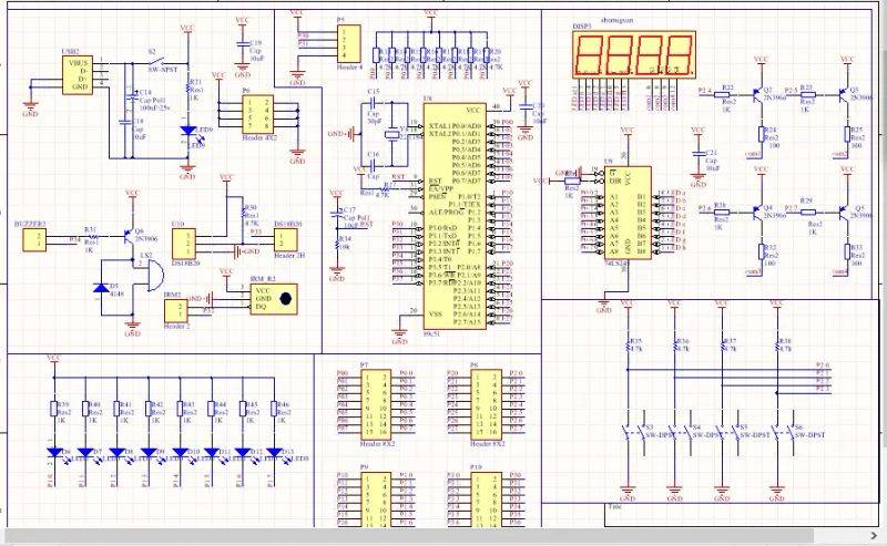
(i) definition of the pcb rationale: the pcb rationale, also known as the circuit logic, is an illustration of the connection between the various elements of the circuit. It does not consider the physical size and location of a metaware, but only the logic and electrical performance of the circuit. Content: the pcb rationale map contains elements such as meta-unit symbols, connection lines and network signs in circuits. A meta-unit symbol indicates electrical resistance, capacitive, sensory, diode, triode, etc. In the circuit; a connection line indicates an electrical connection between the elements; a network sign is used to identify the same connection points in the circuit. Impact: the main role of the pcb rationale map is to help engineers understand the working principles and performance of the circuit, as well as to conduct circuit analysis and design. It was one of the first documents to emerge from the development of electronic products, providing a basis for subsequent pcb design。
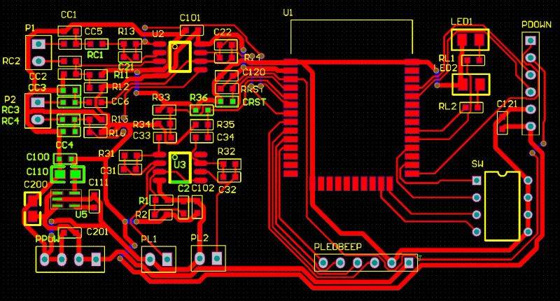
Pcb design document definition: pcb design document means a detailed graphic and data document to guide pcb manufacture and assembly. It contains information on the physical physical dimensions, location, wiring, etc. Of a metaware. Content: the pcb design documents contain elements such as packaging of metaware, wiring layers, welding plates, perforations, silk layers, etc. The packaging of a metaware means the physical size of a metaware and the drawing of its feet; the wiring layer is used to describe the direction and width of the steering line on the circuit board; the welding plate is the point of connection between the feet of a metaware and the steering line of the circuit board; the perforation is used to achieve electrical connections between the different wiring layers; the wiring layer is used to indicate the name, symbol, etc. Of the element on the circuit board. Role: the main role of the pcb design document is to guide the pcb's manufacturing and assembly process. It is a key link in transforming the rationale map into a physical circuit board, which directly determines the performance and reliability of electronic products. Distinctions and linkages: there is a clear difference between the pcb rationale and the pcb design document in terms of definition and content. The pcb rationale map focuses on the logical relationship and electrical performance of the circuit, while the pcb design document focuses on the physical size, location and wiring of the metaware. In addition, the roles of the two are different, with pcb rationale maps being used mainly for circuit analysis and design, while pcb design documents are used mainly to guide pcb manufacture and assembly. Linkages: although the pcb rationale and pcb design documents differ in content and role, they are closely linked. The pcb rationale map, which is the basis for the development of electronic products, provides information on the logic and electrical performance of circuits for subsequent pcb designs. The pcb design document, on the other hand, is a key element in the transformation of the doctrine map into a physical circuit board, which requires the design of metaware layout, wiring, etc., as required by the rationale chart. As a result, both are mutually reinforcing in the development of electronic products。