

Manpower is the fundamental factor in determining the success of projects and opening up industry gaps。
Simulation of the design and production costs of asic can be divided into three core blocks: human costs, software tool costs and sample stream manufacturing costs. While these three plates are equally critical to the success of the project, one point that needs to be focused on is that design tools and crystal-circle-generation plants are common resources in the industry and are equally accessible to all semiconductor enterprises. Simulations of asic have performance problems, which are rarely caused by design tools or by the clipwork。
Human costs: a central factor in bridging the gap
If you plan to study the simulation of asc, specification programming, circuit design and layout are the most critical links. It is also a central watershed that distinguishes between truly self-researched firms and simple windmills。
The above-mentioned links require a high degree of competence in modelling design. The research and development team described here is a senior engineer with hundreds of complex, high-precision simulation chip landing experiences who are able to capture technical indicators that the industry has recognized as unattainable. Such practitioners generally have more than 30 to 40 years of experience, with an annual salary of over $350,000. Such talent is scarce and costly to use, but it is worth every penny。
A central conclusion is that it is human resources that determine the success of the project and open up the gap between industries。
Feasibility study: reducing design risks
The first step in the development of the chip was the feasibility study carried out by the engineer responsible for the chip, and the complete process is illustrated in figure 1 below。
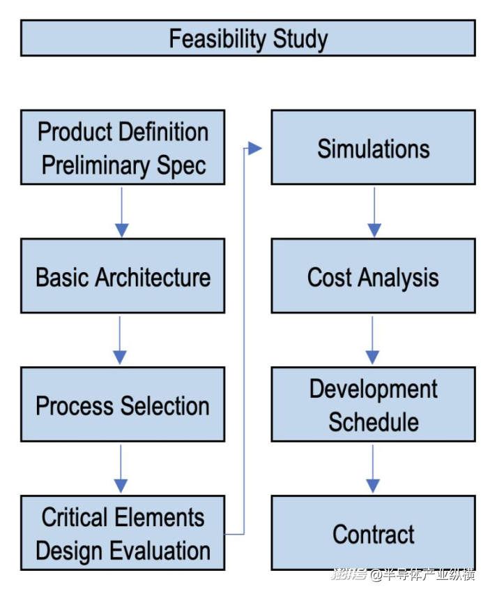
Figure 1 feasibility studies have to be completed under the lead of chip owner design engineers
The feasibility study is a risk-averse process aimed at identifying, quantifying and developing a corresponding mitigation programme to guarantee the successful landing of the project. At the same time, the design team will be able to calculate the overall design cycle through this link and finalize the fixed total development cost。
A feasibility study takes up to two months if the process is complete; a longer cycle if the project contains a large amount of original technology development; and a shorter cycle if the chip only integrates existing mature silicon ips. The cost ranges from $20,000 to $70,000, which is accounted for in the total development cost if a formal development contract is concluded between the two parties. Simulation work is required in the course of the study, which results in high user fees for software tools at the beginning of the project。
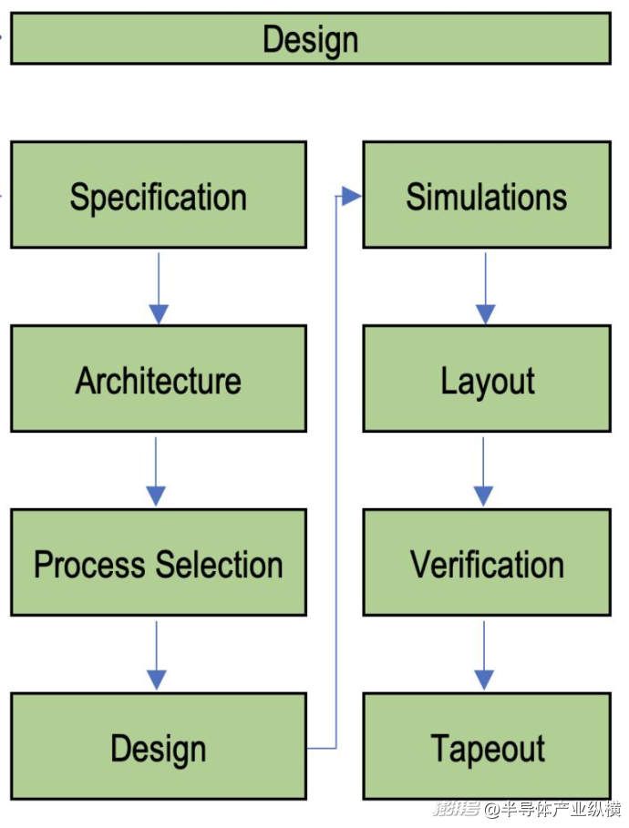
Figure 2
Design phase: from first draft specifications to chip structure landing
The design phase contains a number of core tasks: the original four- to six-page version of the first draft specifications for the product definition, which will be expanded to a complete specification manual of over 50 pages, detailing the parameters at the lower and upper limits, the definition of the repository, the cost of effort criteria, etc。
The level of refinement of the specifications manual is a direct reflection of the professionalism of the design team. The manual will serve as the selection basis for the best-fit round plants and exclusive processes that match the indicators of the suitable chip voltage, current, noise, accuracy, cost, etc。
The team defines the overall asc structure in terms of functional modules and arranges for the development of decades-old engineers of deep-tilled matching modules, covering such modules as charge pumps, 24-bit and above-module converters, high-precision cryogenic reference voltage sources, behead wave stabilization amplifiers, etc. Where conditions permit, the design increases the memory programmability, optimizes the normal distribution of parameters and maximizes the yield of the chip。
Multi-stakeholder collaboration, evaluation and design of control mechanisms
The project arranges weekly on-line communication meetings with client engineers to synchronize project progress, while providing multiple optimisation programmes to achieve such optimization objectives as chip performance enhancement, chip size reduction (reduction in costs), suppression of environmental interference (electric noise, temperature fluctuations), and extension. Upon completion of each core function module, the client engineering team will be required to conduct a dedicated design review to dismantle the entire working method of the module from the transistor level, and the evaluation material will include a chart of circuit principles, simulation indicators and specifications requirements, and a list of supporting peripheral elements。
Harmonization of procurement of full design software tools during the project cycle; quarterly meetings with client enterprise management to synchronize project scheduling and fund utilization; and formation of digital teams for logical, storage, repository-related development。
Testing programme: third-party testing platform vs customized testing system
The design work for the asic chip synchronized propulsion test system development. High-precision simulations of asic tests are difficult, sometimes not less than the development of the chip itself, and the industry is divided into two main realization lines: the first, the output of exclusive test specification documents, is submitted to a third-party test agency, depending on its commercial standardized test equipment. The third party will recommend a suitable test machine model based on the specifications and will charge a one-time development fee for the development of a dedicated hardware and accompanying testing procedure for fit for the asc. Landing costs for the full package are generally between $100,000 and $200,000。
Javier uses the second option: customizing an exclusive testing system that fully matches the asc test requirements. We'll build two identical test devices, one for the crystal probe test and one for the end of the finished product after sealing. Equipment may be deployed to any third-party testing facility, matched by automatic up-to-down platform use, or operated independently。
We prefer the formula because it ensures that the crystal probe test is fully matched to the end-of-life data; and, unexpectedly, the overall cost is lower. The programme has the flexibility to move testing sites without having to repeat the cost of testing equipment。
Customization of ascc versus cost logic for standardized commercial chips
Standardized simulated semiconductor manufacturers develop generic chips for sale to thousands of different customers, with enterprises covering the full cost of their own development and sharing the cost of r & d to the single cost. Enterprises rely on the market sector to forecast sufficient sales to cover r & d inputs over the long term and to make a profit。
However, the business model for the customization of asic is completely different: the project has a single client, who bears the full development cost in exchange for exclusive access to the chip。
Exclusive property rights are essential: clients are willing to bear the costs of r & d, often in order to integrate their own intellectual property rights, develop new technologies, and create performance advantages over out-of-pocket standard devices; in addition, customized asic has multiple advantages such as significantly reduced chip size, lower utility, and risk of avoiding the cut-off of a metaware。
Software tools: powerful but costly to use
The total cost of developing integrated circuits includes the cost of making and encapsulating crystal circles, and here we focus on the two main costs of manpower and software tools, which hide a number of easily neglected expenses. Those who are not familiar with the chip development process are often under pressure to see the associated cost figures。
The semiconductor industry often focuses on the billions of dollars in capital costs of the advanced digital process, but the cost logic of modelling chip development is quite different: no large production equipment inputs are required, and core costs are concentrated on human and tool-authorized leasing。
Simulation applications such as automobiles electronics, consumer electronics, sensor calibration and signal reconciliation, which have erupted over the past decades, have facilitated the cross-up upgrading of simulation chip design tools, which require high levels of precision, quality and reliability. The mainstream tools for simulating engineers include the role models virtuoso and spectre, new think technologies primetime, and the guide calibre。
Regardless of which manufacturer you choose to develop the simulation asc, the basic tools used are the above-mentioned generic tools, which can be purchased across the industry. However, the instruments are authorized to be expensive and the costs must be included in the budget. Officially unpricing, and confidentiality agreements prohibit disclosure by users, industry estimates a complete set of analogue/mixed signal design authorizations (support mapping and circuit simulations) between us$ 150,000 and us$ 300,000 per year. The set of authorizations is available on-line only for one person, with significant incremental costs。
Cost of sample stream and mask
The vast majority of the rounding plants have introduced multi-project round (mpw) services for their own processes, which provide a high-quality channel for the validation of silicon samples from low-cost stream films, enabling them to locate prenatally and repair various design deficiencies。
Mainty processes open multi-project crystal stream films once a month; small-scale processes are less frequent, two to six times a year. If you miss the stream window period, you have to wait for a longer period. The multi-project crystal circle is not a mandatory link development, but it is a key step in the pre-natal verification of early silicon chips, debugging testing systems, when conditions permit。
Whether or not a multi-project crystal circle is used, the largest process in the mass production phase costs a full set of photomass at a price varying from $75,000 to $150,000 for the total number of photomass required for the crystal mill and chips。
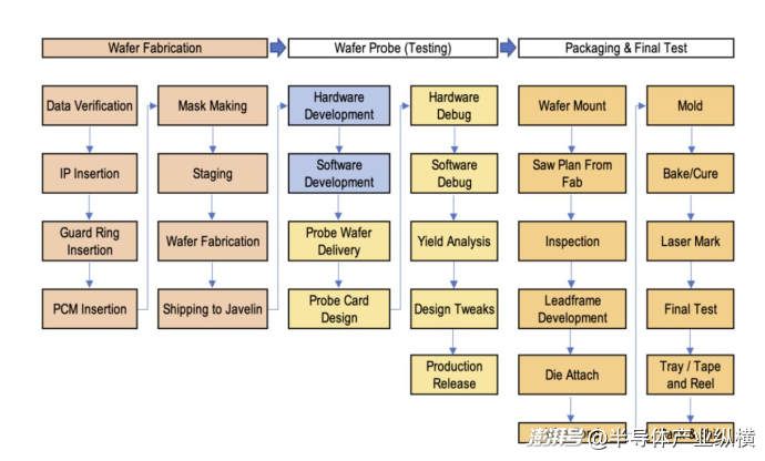
Figure 3 tests and seals are an important part of the asc manufacturing costs
Experience determines success or failure: managing ascic development risks
In case of design problems with standardized commercial chips, the semiconductor may delay listing and arrange for engineer restoration problems. However, the customization of asic does not have buffer space: customers need chips delivered at established nodes to support the marketing of a new generation of products。
It is important not to lose faith in the fact that an enterprise claims 20 or 30 years of business history and that the reference value of a business life is extremely low, depending on the practical experience of a front-line research and development worker. How many years has each engineer had to model an asc independent design experience
All people make mistakes, but mistakes are learning processes. The team you need is a senior engineer who stepped on the same pit decades ago and settled mature solutions, so that your project does not become a new man's practice. You have the right to have access to the full curriculum vitae of the engineer in charge of the project, to request a review on your own initiative and to apply for direct communication with the engineer。
This leads to another point: you should have direct access to all engineers involved in the development of this chip and not accept project managers or market people as the only communication barrier. Such personnel do not have the specialized technical capacity to extend communication links, and most of the chip projects are highly sensitive to time nodes。