

In all types of motor electronics controls, boost is often designed to ensure that some functions can still be operated after the voltage has dropped to a certain value。
Boost is a switch source that maintains a steady output using the time ratio of switch openings and switches. It is widely applied in electronics in industries with small, light and efficient characteristics and is an indispensable power structure。
1. Structures
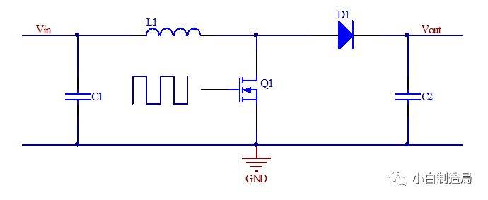
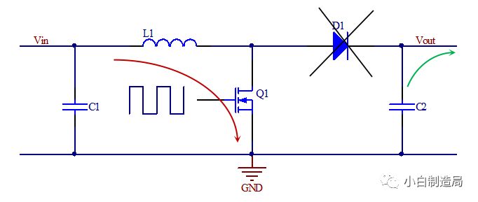
The following is the boosst circuit extension structure, the main components of which are mos tubes, electrons, diodes, each with a number of electric caps. General small-power boost type dcdc chip l1 and d1 external, large-power dcdc chip mos tube external. Controls mos conduits and off using pwm。
2. Mos pipe conductor (charging process)
After the mos cathetering, the current flows to the following graph red arrows, and the sense starts charging and converts to magnetic energy, at which point the diode is closed and the output energy is all provided by the c2 caps, as follows。
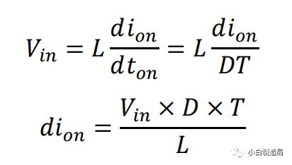
Switch lead time = space ratio * switch cycle = d*t。
3, mos pipe shut down (discharge process)
Following the closure of the mos tube, the current flows to the following map green arrows, which release energy from the electric sensor, when the electrical sense is like a battery and vin combines to power the load while charging the output cap c2. At this point, the load is provided by the output capacitor c2 and the diode d1. D1 generally selects the shortki diode, which leads to rapid and low-intensity transport。
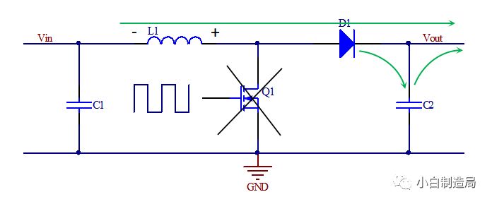
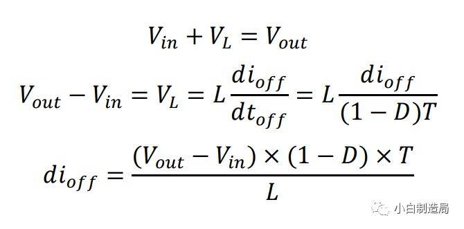
Time of discharge = (1-to-empty)* switch cycle = (1-d)*t. At this point, vin, together with the telepathic l1, discharges the load, so that the positive and negative numbers are not confused (as shown above, the two are overlapping)。
4. Pressure formula
Based on the volt-sec properties of the sensor: the charge and discharge are the same for two periods of open-off and disconnection. There are:
That is:

Once organized, the following can be obtained:
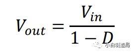
According to this formula, we can clearly know that the lifting factor is determined by the pwm ratio. When d=0. 5, the output is twice the input。
5. Chip applications
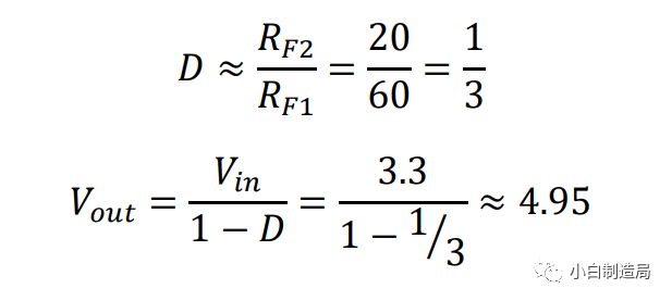
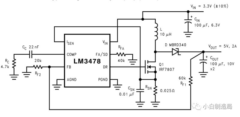
For example, ti's lm 3478 (2. 97v ~ 40v wide input range boost) chip, fb voltage is 1. 26 v for applications such as: