The challenge to industrial lenses is only just beginning when the sensor becomes more and more like a dollar。
As the consumer electronics, new energy sources and the automobile industry's extreme pursuit of detection accuracy, industrial cameras are rapidly entering the “high pixel age”. 60 million, 150 million or more pixels are becoming increasingly common. However, many engineers found that the problem of vagueness and uneven brightness on the edges of the images had become more pronounced when these “super cameras” had been fitted into the lenses, and that the increase in resolution had not led to the desired improvement in clarity。
The root of the problem is that high pixels not only mean smaller pixel sizes, but are often accompanied by an increase in the target surface of sensors. In order to manage such sensors, a single lens must be accompanied by three major examinations: covering large target surfaces, matching high resolution, and ensuring parity across the field of view。
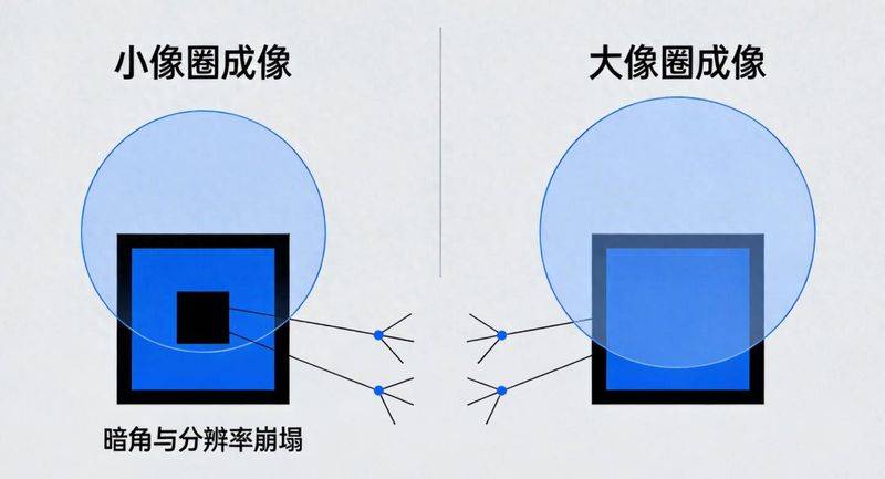
Challenge one: field cover -- the canvas gets bigger and the edges don't go away
Larger sensors (e. G., 1. 1 inches, full picture) require lenses to provide greater clarity. Images traditionally designed for smaller target surfaces (e. G., 2/3 inches) cover only the central area of a large sensor, leading to a severe drop in the “crawl” of dark angles, resolution and contrast at the edge。
Technical nature: the light from the edges of the field of view enters with a larger angle, making it easier to produce off-axis images, such as dispersing, syllables, comets, etc. Correcting these weaknesses requires more sophisticated optical designs。
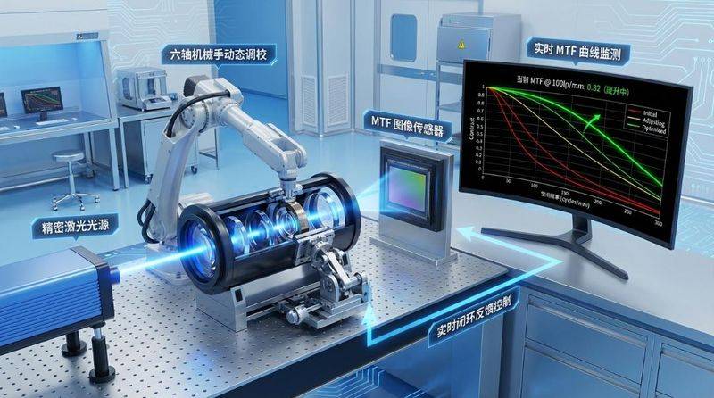
激: our optic design team's primary task in the design of large target lenses is to simulate accurately and optimize the optical trajectory of the outer field of view through software simulation. This usually requires the use of more mirror groups, non-spherical mirrors and even abnormally dispersed glass for efficient correction. For example, in the large target lens project customised for a screen visual detection device, we have succeeded in increasing the contrast of the 1. 1-inch sensor's most extreme angle from less than 60 per cent of conventional designs to more than 85 per cent by introducing two precision model-pressed non-spherical mirrors, while maintaining the mtf values of the edges at the service level, meeting the customer's stringent requirements for full screen equilibration。
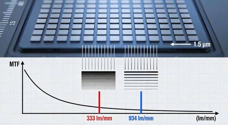
Challenge two: resolution matching - "systems" more subtle, testing real kung fu
High pixel cameras can be as small as 1. 5 μm or even smaller. According to the nyquist sampling theorem, the lens would need to maintain a significant mtf value at a spatial frequency above 300 lp/mm in order to be truly “saturated”. This imposes nanoscale requirements for lens design limits, material balance and calibration precision。
Technical nature: it's close to the limit of optical diffusion. Any small pre-wave error (sourced from design residue, material imbalance, load bias) is sensitively reflected in mtf decline。
Indo-ete practice:
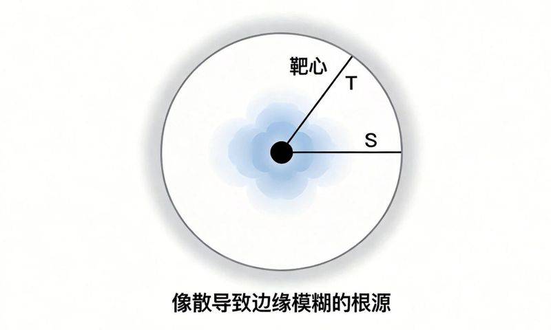
Material-level screening: we conduct pre-wave interferometric screening of optical glass used for high-resolution lenses, remove internal graphy or uneven refractive embryos and control pre-wave malformations from the source. Public-level control and pro-active targeting: the public-pattern differential of the lens is compressed to the micrometre level. We use a proactive alignment process to monitor mtfs in real time at the centre and in multiple off-axis sights during mirror assembly, and dynamically adjust the position of the lenses to ensure that the actual performance of each lens is close to the best design value, rather than simply “falling into the public belt”. Provides a factual report of “sensor matching”: using mtf testers with large sensor simulators, we conduct measurements at multiple visual sites (centre, 0. 7 visual field, 0. 9 visual field, full angle) and provide reports containing detailed data within the sensor size of the client camera. We believe that measured data on the full range are more of reference value than a single central theoretical resolution value. Challenge three: like differential control and consistency - the “tests field” is stronger and even is key
Any difference is magnified under large target surfaces and high resolution. Fragmentation of the edge vision field may result in different claritys of the same feature in the midday and arc vector directions, which seriously affect the consistency of measurement and identification。
(a) stimulate the ette practice: we respond through the optimal design of multi-purpose constraints:
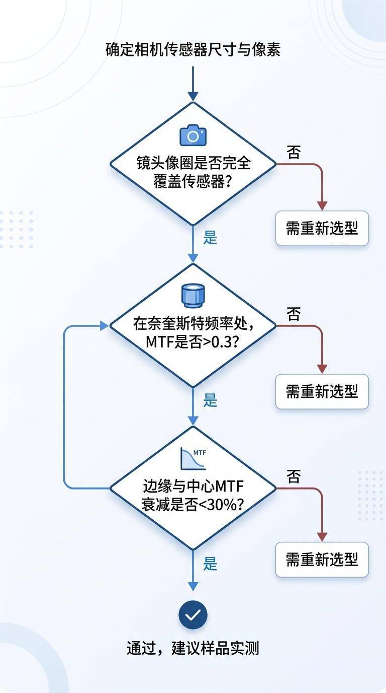
Field selection guide: the primary matching sensor size for a high pixel system must be greater than the size of the sensor for your camera. A mtf curve to match the sensor: the supplier is required to provide an mtf curve that covers the full opposite dimensions of the sensor you use. Focus has been placed on the extent of mtf decline in high frequency (hf) locations in the 0. 7 and 100 per cent (especially at the corner). The less decay, the better. Calculate and validate resolution matching: critical spatial frequencies based on camera pixel size (10001000/(2*pixel size μm)). View the value of the lens mtf curve at that frequency, preferably >0. 3,0. 7 on the axis should not be less than 0. 2. Focus on the balance of colour and light: ask about the relative light curve and colour correction of the lens under the spectrum band you use (e. G., white light, specific monochrome). For detection applications, homogeneity is often more important than maximum resolution. Be wary of “over-resolution” and the cost trap: if your application is a defect recognition rather than a submaritic dimension measurement, a medium-resolution, but well-balanced lens with a suitable working distance may be a more stable and economical option. Engineers who stimulate etv are happy to assist you in this kind of value analysis。
Controlling high-pixel cameras is a comprehensive examination of lens optical design, material science, precision manufacturing and detection capabilities. Electromagnetic power is dedicated to providing customers with optical solutions that truly release the potential of high pixel sensors through solid simulation designs, nanoscale process management and realistic testing, making each pixel a reliable courier and delivering clear visual truth。
This paper was compiled by the technical team of nanjing tweet optical electronics ltd. And is based on optical engineering principles and our practice in high-resolution imaging projects. We can provide lens selection analysis, matching tests and customized development services for high pixel visual systems, and welcome communication。